Wet method etching process

A wet etching and process technology, applied in the field of solar cells, can solve the problems of reducing quantum efficiency in the long-wave band, increasing back recombination, and reducing Isc, and achieves the effects of increasing Voc, strengthening back reflection, and increasing Isc

Inactive Publication Date: 2012-07-11
HEFEI & SOLAR TECH
View PDF5 Cites 15 Cited by
  • Summary
  • Abstract
  • Description
  • Claims
  • Application Information

AI Technical Summary

Problems solved by technology

Moreover, the rough back surface has a larger surface area, which will increase the recombination on the back, reduce the internal quantum efficiency in the long-wave band, and reduce the Isc

Method used


Image

  • Wet method etching process
  • Wet method etching process
  • Wet method etching process

Examples


Embodiment 1

[0025] The wet etching process of the crystalline silicon wafer provided in this embodiment comprises the following steps:

[0026] (1) Select cells after doping and diffusion treatment;

[0027] (2) Etch the above cell to remove the surrounding PN junction, etch by chain wet etching, using 3% HF and 40% HNO by mass percentage 3 Mix the solution to remove the PN junction around the silicon wafer;

[0028] (3) Polish the backside of the cell with the peripheral PN junction removed at 5°C for 10 seconds using a polishing solution. The polishing solution used contains the following components in mass percentage: HF10%, HNO 3 55%, H 2 SO 4 10%, acetic acid 5%, and additives ammonium fluoride, potassium nitrite, potassium sulfate 10%;

[0029] (4) 10% HF is used to remove phosphosilicate glass PSG;

[0030] (5) Dry the above-mentioned cell sheets by air drying.

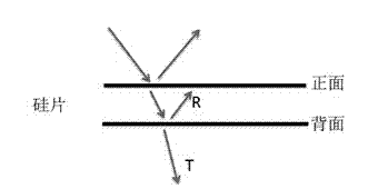
[0031] Such as figure 1 As shown in , after removing the edge junction, increasing the back polishing process c...

Embodiment 2

[0033] The wet etching process of the crystalline silicon wafer provided in this embodiment comprises the following steps:

[0034] (1) Select cells after doping and diffusion treatment;

[0035] (2) Etch the above cell to remove the surrounding PN junction, etch by chain wet etching, using 3% HF and 40% HNO by mass percentage 3 Mix the solution to remove the PN junction around the silicon wafer;

[0036] (3) Remove phosphosilicate glass PSG by mass percentage content 5% HF;

[0037] (4) Polish the backside of the cell with the peripheral PN junction removed at 30°C for 10 minutes with a polishing solution. The polishing solution used contains the following components in mass percentage: HF 0.5%, HNO 3 5%, H 2 SO 4 50%, acetic acid 30% and additives potassium nitrite, potassium citrate, potassium lauryl sulfate 10%;

[0038] (5) Dry the above-mentioned cells by spinning.

[0039] Such as figure 1 As shown in , after removing the edge junction, increasing the back poli...

Embodiment 3

[0042] The wet etching process of the crystalline silicon wafer provided in this embodiment comprises the following steps:

[0043] (1) Select cells after doping and diffusion treatment;

[0044] (2) Etch the above-mentioned cells to remove the surrounding PN junctions, and dry plasma etching is used for etching;

[0045] (3) 20% HF by mass percentage is used to remove phosphosilicate glass PSG;

[0046] (4) Polish the backside of the cell with the peripheral PN junction removed at 15°C for 5 minutes using a polishing solution. The polishing solution used contains the following components in mass percentage: HF 1%, HNO 3 30%, H 2 SO 4 5%, acetic acid 25% and additives ammonium fluoride, potassium nitrite, potassium citrate, potassium lauryl ether phosphate and potassium lauryl sulfate 20%;

[0047] (5) Dry the above-mentioned cell sheets by air drying.

[0048] Such as figure 1 As shown in , after removing the edge junction, increasing the back polishing process can ma...


PUM


Abstract

The invention discloses a wet method etching process for crystal silicon wafers, which mainly comprises a back side polishing process. After etching and edge removing, the polishing process performed to the back sides of the crystal silicon wafers through a polishing solution is added, the temperature of the polishing solution in polishing is 5-30 DEG C, the polishing time is 10 seconds to 10 minutes, and the polishing solution contains, by mass, 0.5%-10% of HF, 35%-55% of HNO, 45%-55% of H2SO4 and 5%-30% of acetic acid. By adding the back side polishing process, the back sides of the silicon wafers can be smooth, back reflection of the silicon wafers is strengthened, and absorption of long-wave band spectrums in sunlight is enhanced, thereby improving light energy conversion and short-circuit current (Isc) of a battery and finally improving the conversion efficiency of the battery. In addition, the back of the smooth battery further facilitates combination of follow-up aluminum-silicon alloy and a silicon body, improves ohmic contact, strengthens the light reflection effect of an interface, improves variable output circuit (Voc), and finally improves the conversion efficiency of the battery.

Description

technical field [0001] The invention belongs to the technical field of solar cells, and in particular relates to a wet etching process. Background technique [0002] The general process of the current commercial crystalline silicon solar cell production is as follows: new single / polycrystalline silicon wafer → removal of the damaged layer on the surface of the silicon wafer, making the textured surface → in POCl 3 Phosphorus diffuses in the atmosphere to form N + Diffusion layer → use etching to remove the PN junction around the silicon wafer → use PECVD technology to deposit SiNx anti-reflection film on the front surface → screen print the back electrode, back electric field, and positive electrode → sinter in the sintering furnace to form an ohmic contact → test points select. This commercial solar cell manufacturing technology is relatively simple and mature, suitable for industrialized and automated production, and thus widely used. [0003] For a long time, silicon m...

Claims


Application Information

Patent Timeline
Patent Type & Authority Applications(China)
IPC IPC(8): H01L31/18C23F1/24
CPCY02P70/50
Inventor 刘光朱生宾王永丰谢忠阳
Owner HEFEI & SOLAR TECH
Why Eureka
Try Eureka