Nitrogen-faced gallium nitride suede solar cell and fabrication method thereof

A technology of solar cells and manufacturing methods, applied in the field of microelectronics, can solve the problems of low photoelectric conversion efficiency and high production costs, and achieve the effects of easy control of corrosion time and temperature, large short-circuit current, and improved performance

Inactive Publication Date: 2014-10-01
XIDIAN UNIV
View PDF3 Cites 0 Cited by
  • Summary
  • Abstract
  • Description
  • Claims
  • Application Information

AI Technical Summary

Problems solved by technology

[0007] Except TiO 2 In addition to two wide bandgap semiconductor materials, ZnO and ZnO, there is also Gallium Nitride (GaN) material developed in recent years, which is a direct bandgap semiconductor with a wide bandgap, high carrier mobility, high thermal conductivity, and high voltage resistance. , high temperature resistance, corrosion resistance, radiation resistance and other outstanding advantages; however, the current hybrid solar cells not only have high production costs, but also have low photoelectric conversion efficiency, and their maximum conversion efficiency is less than 40%.

Method used


Image

  • Nitrogen-faced gallium nitride suede solar cell and fabrication method thereof
  • Nitrogen-faced gallium nitride suede solar cell and fabrication method thereof

Examples


Embodiment 1

[0028] Embodiment 1, comprises the steps:

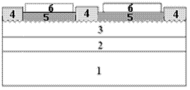
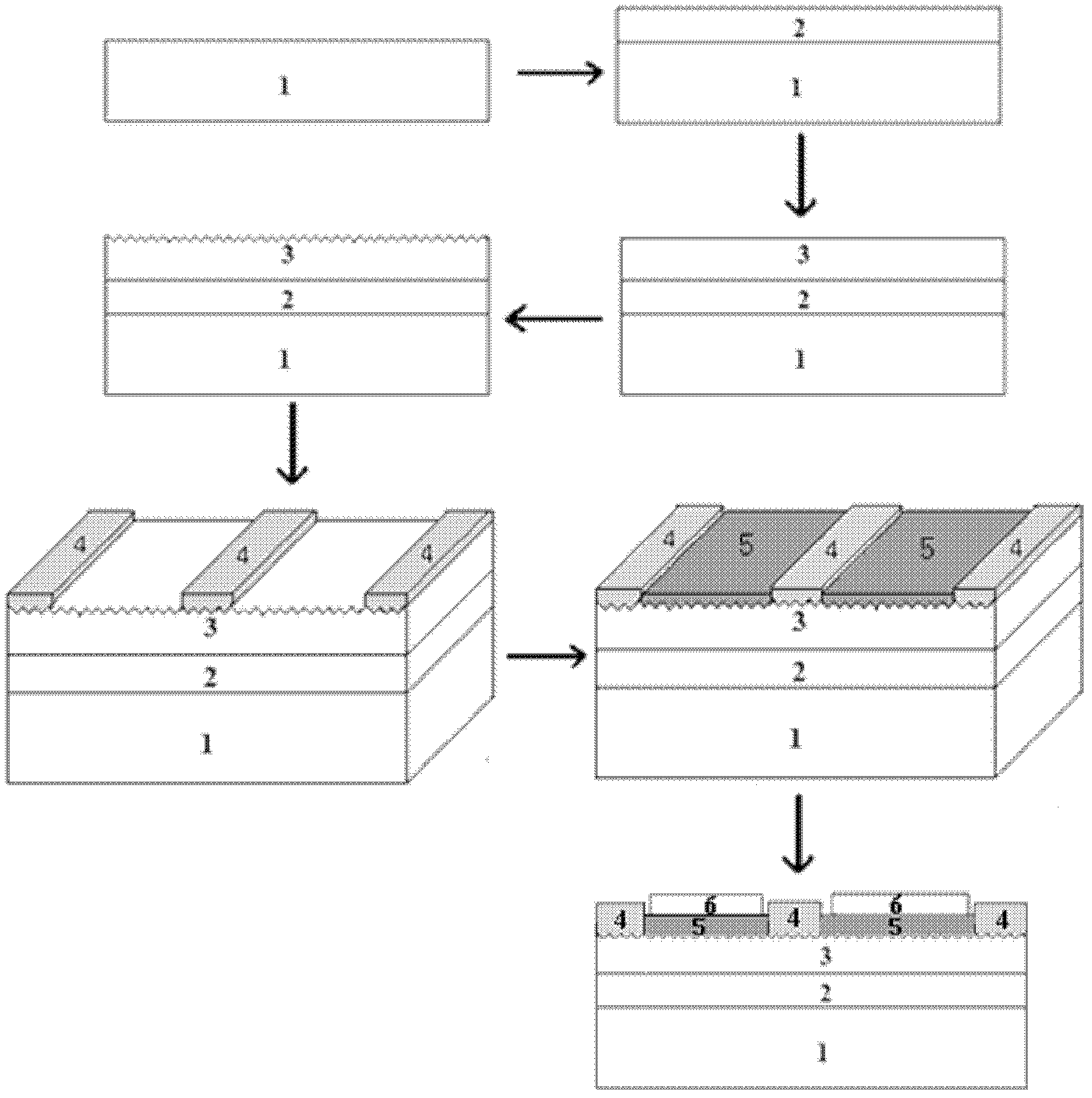
[0029] Step 1, grow an AlN buffer layer with a thickness of 150nm on the sapphire substrate by MOCVD method, and the process conditions are: temperature is 1050°C, NH 3 It is 3500sccm, TMAl is 30sccm, and the time is 30min.

[0030]Step 2: On the AlN buffer layer, the MOCVD method is used to grow the thickness of 2 μm and the electron concentration of 1.0×10 17 cm -3 -2.0×10 18 cm -3 The nitrogen surface n-GaN epitaxial layer, the process conditions are: the temperature is 1020 ℃, NH 3 It was performed at 5000 sccm, TEGa at 220 sccm, and for 2 hours.

[0031] Step 3, put the sample material after growing the n-GaN epitaxial layer on the nitrogen surface into acetone and absolute ethanol for 3 minutes, respectively, and ultrasonically clean it for 3 minutes, repeat twice, and then use deionized water to clean it ultrasonically for 10 minutes.

[0032] Step 4, add KOH solution with a concentration of 15% into the beaker, heat it ...

Embodiment 2

[0036] Embodiment 2, comprises the steps:

[0037] Step 1, at a temperature of 1050°C, NH 3 Under the process conditions of 3500 sccm, 30 sccm of TMAl, and 30 min, an AlN buffer layer with a thickness of 150 nm was grown on the sapphire substrate by MOCVD method.

[0038] Step 2, using MOCVD method, at a temperature of 1020 ° C, NH 3 Under the conditions of 5000 sccm, TEGa 220 sccm, and a time of 2 hours, the growth thickness on the AlN buffer layer is 2 μm, and the electron concentration is 1.0×10 17 cm -3 -2.0×10 18 cm -3 The nitrogen-faced n-GaN epitaxial layer.

[0039] Step 3, put the sample after growing the n-GaN epitaxial layer on the nitrogen surface into acetone and absolute ethanol for 3 minutes for ultrasonic cleaning respectively, repeat twice and then use deionized water for 15 minutes for ultrasonic cleaning.

[0040] Step 4: Add the prepared KOH solution with a concentration of 20% into the beaker, heat it to 85°C with a universal heating furnace, measure...

Embodiment 3

[0044] Embodiment 3, comprises the steps:

[0045] In step A, an AlN buffer layer with a thickness of 200nm is grown on a sapphire substrate by MOCVD, and the growth process conditions are as follows: temperature is 1050°C, NH 3 It is 3500 sccm, TMAl is 30 sccm, and the time is 40 min.

[0046] Step B, using MOCVD to grow on the AlN buffer layer with a thickness of 3 μm and an electron concentration of 1.0×10 17 cm -3 -2.0×10 18 cm -3 The nitrogen surface n-GaN epitaxial layer, the process conditions are: the temperature is 1020 ℃, NH 3 It is 5000 sccm, TEGa is 220 sccm, and the time is 3 hours.

[0047] In step C, the sample material after growing the n-GaN epitaxial layer on the nitrogen surface is put into acetone and absolute ethanol for 3 minutes, respectively, and ultrasonically cleaned for 3 minutes, and after repeated 2 times, ultrasonically cleaned with deionized water for 12 minutes.

[0048] Step D, add the prepared KOH solution with a concentration of 25% int...


PUM

PropertyMeasurementUnit
thicknessaaaaaaaaaa
depthaaaaaaaaaa
depthaaaaaaaaaa

Abstract

The invention discloses a nitrogen-side gallium nitride napped-side solar battery and a production method thereof, which mainly solve the problems of the present solar battery that the efficiency is low and the cost is high. The nitrogen-side gallium nitride napped-side solar battery comprises a sapphire substrate (1), aluminum nitride (AlN) buffering layer (2), an extension layer (3), a cathode (4), an organic polymer layer (5) and an anode (6), wherein the AlN buffering layer (2) adopts metal-organic chemical vapor deposition (MOCVD) growth, and the thickness is 150nm to 200nm; the extension layer (3) adopts a nitrogen surface n-GaN grown by the MOCVD with the thickness of 2 to 3 micrometers and the electronic density of 1.0*1017cm<-3> to 2.0*1018cm<-3>, the surface which is contacted with the organic polymer layer (5) is a recess napped surface, the density of the recesses is 1.0*107cm<-2> to 4.0*108cm<-2>, and the depth is 450 nm to 1.5 micrometers; the cathode (4) is formed by depositing titanium (Ti) and aluminum (Al) on the nitrogen side n-GaN layer; the organic polymer layer (5) is formed by spin coating on the surface of the nitrogen side n-GaN layer, and the thickness is 50 to 80nm; and the anode (6) is formed by depositing gold Au on the organic polymer layer (5). The process is simple, the cost is low, the photoelectric conversion efficiency is high, and the nitrogen-side gallium nitrode napped-side solar battery and the production method can be used for the commercial and civil power generation systems.

Description

technical field [0001] The invention belongs to the technical field of microelectronics, and in particular relates to a solar cell, that is, a gallium nitride textured solar cell on a nitrogen surface. Specifically, a nitrogen-faced n-GaN layer with a crystal orientation of [0001] is grown on sapphire, and the surface of the nitrogen-faced GaN is textured using a diluted KOH solution, and spin-coated on the textured GaN surface. A layer of organic conductive film forms an excellent Schottky contact to realize photovoltaic characteristics. technical background [0002] On the one hand, the development of modern industry has increased the demand for energy, causing an energy crisis; on the other hand, a large amount of carbon dioxide gas has been released in the use of conventional energy, leading to a global "greenhouse effect". To this end, countries are trying to get rid of the dependence on conventional energy, and accelerate the development of renewable energy, as a very...

Claims


Application Information

Patent Timeline
Patent Type & Authority Patents(China)
IPC IPC(8): H01L51/42H01L51/46H01L51/48
CPCY02E10/549Y02P70/50
Inventor 冯倩李倩郝跃邢涛王强
Owner XIDIAN UNIV
Why Eureka
Try Eureka