
Silicon-based heterojunction double-side solar cell and preparation method thereof

A solar cell and heterojunction technology, applied in circuits, photovoltaic power generation, electrical components, etc., can solve problems such as collection obstacles, large energy band mismatch, and unfavorable collection, and achieve the effects of reducing series resistance and improving conversion efficiency

Active Publication Date: 2012-10-17
(CNBM) BENGBU DESIGN & RES INST FOR GLASS IND CO LTD +1
View PDF5 Cites 11 Cited by
  • Summary
  • Abstract
  • Description
  • Claims
  • Application Information

AI Technical Summary

Problems solved by technology

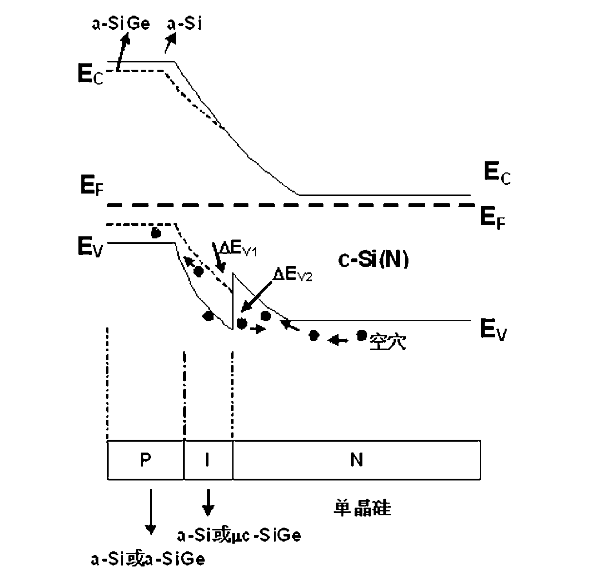
This kind of battery product, including the designs carried out by many international research institutions, uses amorphous silicon thin film as the emitter of the battery to form a heterogeneous PN junction, collect photo-generated carriers and generate photovoltaic effect, but this design The disadvantage is that the energy band mismatch between the emitter amorphous silicon and the base crystalline silicon is large, and the resulting energy gap barrier hinders the collection of photogenerated minority carriers, which is not conducive to collection, thus affecting Its photovoltaic performance

Method used


Image

  • Silicon-based heterojunction double-side solar cell and preparation method thereof
  • Silicon-based heterojunction double-side solar cell and preparation method thereof
  • Silicon-based heterojunction double-side solar cell and preparation method thereof

Examples


Embodiment Construction

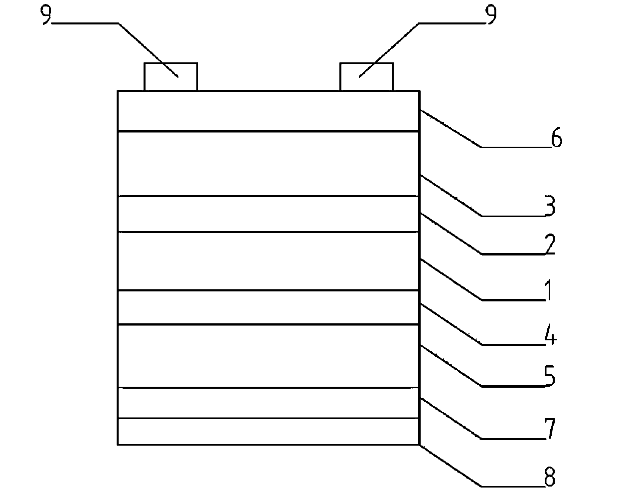
[0029] (1) The standard cleaning procedure for silicon wafers, that is, the RCA cleaning process, is used for standard cleaning of the N-type double-sided polished single crystal silicon wafer 1 produced by the FZ method. In the experiment, the thickness of the N-type double-sided polished single crystal silicon wafer 1 is selected. It is 0.220mm, the conductivity is 1~2S / cm, and the area is 4cm 2 (a square with a side length of 2 cm);

[0030](2) Immerse the cleaned N-type double-sided polished single crystal silicon wafer 1 in a hydrofluoric acid aqueous solution with a concentration of 2%, and keep it for 10 seconds to ensure that the silicon dioxide oxide film on the surface of the single crystal silicon is removed, and at the same time It will not cause excessive etching of the silicon surface by hydrofluoric acid. Then quickly put the processed N-type double-sided polished single crystal silicon wafer 1 into the vacuum chamber, draw a high vacuum, and set the substrate ...


PUM

PropertyMeasurementUnit
Thicknessaaaaaaaaaa
Widthaaaaaaaaaa
Thicknessaaaaaaaaaa

Abstract

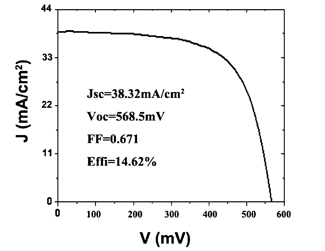
The invention discloses a silicon-based heterojunction double-side solar cell and a preparation method of the silicon-based heterojunction double-side cell. The conventional amorphous-silicon thin-film is replaced by the amorphous-silicon germanium alloy as an emitting diode of the heterojunction cell, at the same time, an intrinsic microcrystalline silicon germanium thin-film is used as an interface buffer layer of the cell, so that valence-band offset caused by the heterojunction band mismatch can be reduced effectively, the block influence on the holes is decreased, and the collection of the photovoltaic minority carrier holes is facilitated, furthermore the photovoltaic performance index of the solar cell is increased. The intrinsic microcrystalline silicon germanium thin film, a P-type doped amorphous-silicon germanium thin film, an intrinsic amorphous-silicon thin-film and an N+ type doped amorphous-silicon thin-film are prepared on two sides of the N-type microcrystalline silicon wafer by the radio frequency plasma enhanced chemical vapor deposition, the purpose of effectively collecting a photovoltaic carrier is achieved. The heterojunction double-side solar cell with 14.62% of photoelectric conversion efficiency is prepared on the double-side polished FZ-type microcrystalline silicon wafer by the process.

Description

technical field [0001] The invention relates to a double-sided heterojunction battery in the field of photovoltaic power generation, in particular to an amorphous silicon germanium / microcrystalline silicon germanium / crystalline silicon heterojunction double-sided solar battery and a preparation method thereof. Background technique [0002] Thin-film silicon / crystalline silicon heterojunction solar cell is a photovoltaic solar cell that combines the respective advantages of the first-generation crystalline silicon cell and the second-generation thin-film cell. It mainly relies on crystalline silicon as the absorbing layer, and the thin-film layer is only for A heterogeneous PN junction is formed to collect photogenerated carriers, so the thickness of the film layer is not high, which makes the light stability of this kind of battery high; at the same time, the battery preparation process is mainly the deposition process of the film, and the process temperature is low, about 18...

Claims


Application Information

Patent Timeline
IPC IPC(8): H01L31/0747H01L31/0352H01L31/028H01L31/20
CPCY02E10/50Y02E10/547Y02P70/50
Inventor 彭寿马立云崔介东王芸
Owner (CNBM) BENGBU DESIGN & RES INST FOR GLASS IND CO LTD
Learn More