High-frequency and low-noise gallium nitride transistor structure with high electronic mobility

A technology of electron mobility and low noise, applied in circuits, electrical components, semiconductor devices, etc., can solve problems such as increasing channel current fluctuations, noise deterioration, and reducing device noise performance, so as to increase saturation rate and mobility, improve Effects of Interface Characteristics and Noise Performance Improvement

Inactive Publication Date: 2013-01-16
UNIV OF ELECTRONICS SCI & TECH OF CHINA
View PDF8 Cites 18 Cited by
  • Summary
  • Abstract
  • Description
  • Claims
  • Application Information

AI Technical Summary

Problems solved by technology

[0003] In the prior art, the transistor structure traditionally used to make GaN low-noise circuit design is as follows figure 1 As shown, the AlGaN (aluminum gallium nitrogen) barrier layer is directly epitaxially grown on the substrate material 4H-SiC, AlN material, and gallium nitride (GaN) buffer layer, and the aluminum composition in the AlGaN barrier layer is 15%~40% Between (see open literature DC, RF, and Microwave Noise Performance of AlGaN–GaN Field Effect Transistors Dependence of Aluminum Concentration Wu Lu, Vipan Kumar, Edwin L. Piner, and Ilesanmi Adesida IEEE TRANSACTIONS ON ELECTRON DEVICES, VOL.50, NO .4, APRIL 2003), such a device structure has the following three main disadvantages in terms of low noise: (1) Since the composition ratio of aluminum atoms and gallium atoms is not the same, aluminum gallium atoms are randomly arranged in the crystal, which is harmful to the presence of The periodic potential field produces perturbation, which induces alloy scattering of carriers, resulting in reduced noise performance of trench devices
(2) Epitaxial growth of the AlGaN barrier layer directly on the GaN buffer layer. During the growth of the GaN buffer layer, due to the process, the grown GaN film has discontinuity and rough surface, which reduces the growth of the AlGaN barrier layer. quality, resulting in more defects in the AlGaN barrier layer, which reduces the transconductance and gain of the device
At the same time, due to the trap effect affecting the lateral movement of the two-dimensional electron gas in the channel, the fluctuation of the channel current is increased and the noise performance of the device is reduced.
(3) During the movement of the two-dimensional electron gas, electrons will directly tunnel into the AlGaN barrier layer, resulting in gate leakage current and noise deterioration

Method used


Image

  • High-frequency and low-noise gallium nitride transistor structure with high electronic mobility
  • High-frequency and low-noise gallium nitride transistor structure with high electronic mobility
  • High-frequency and low-noise gallium nitride transistor structure with high electronic mobility

Examples


Embodiment Construction

[0014] The present invention will be further described below in conjunction with the accompanying drawings and specific embodiments.

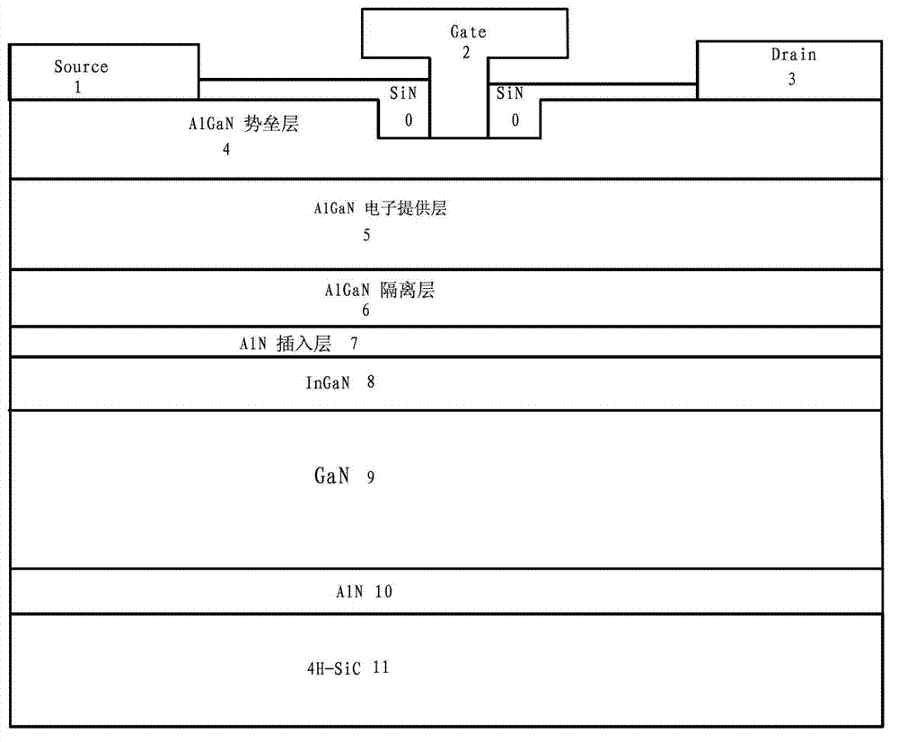
[0015] Such as figure 2 The specific embodiment shown is a high-frequency, low-noise gallium nitride-based high electron mobility transistor structure, including a substrate 11 stacked sequentially from bottom to top, an aluminum nitride (AlN) component on the substrate 11 The core layer 10, the gallium nitride (GaN) buffer layer 9 located on the aluminum nitride nucleation layer 10, the gallium nitride (GaN) buffer layer 9 is further stacked with indium for improving the roughness of the device interface Gallium nitride (InGaN) insertion layer 8, aluminum nitride (AlN) insertion layer 7 for increasing the potential barrier, aluminum gallium nitride (AlGaN) isolation layer 6, aluminum gallium nitride (AlGaN) electron supply layer 5, aluminum gallium nitride ( AlGaN) barrier layer 4 and source 1 , gate 2 and drain 3 respectively connected to t...


PUM

PropertyMeasurementUnit
thicknessaaaaaaaaaa
thicknessaaaaaaaaaa
thicknessaaaaaaaaaa

Abstract

The invention relates to a high-frequency and low-noise gallium nitride transistor structure with high electronic mobility. The structure comprises a substrate, an aluminium nitride nucleating layer arranged on the substrate and a gallium nitride cushioning layer arranged on the aluminium nitride nucleating layer; the substrate, the aluminium nitride nucleating layer and the gallium nitride cushioning layer are sequentially overlapped from bottom to top; the high-frequency and low-noise gallium nitride transistor structure with the high electronic mobility is characterized in that an InGaN inserting layer for improving roughness of a component interface, an aluminium nitride inserting layer for improving a potential barrier, an AlGaN isolating layer, an AlGaN electronic providing layer, an AlGaN potential barrier layer as well as a source electrode, a grid electrode and a drain electrode which are respectively in ohm connection with the AlGaN potential barrier layer are sequentially overlapped on the gallium nitride cushioning layer. The high-frequency and low-noise gallium nitride transistor structure has the beneficial effects that two-dimensional electronic gas is better bound in a potential well, therefore, scattering of the two-dimensional electronic gas caused by impurities in a channel layer is reduced, and a saturated rate and a mobility ratio of the two-dimensional electronic gas are increased, and a noise performance of a device is improved, particularly a high-frequency noise performance.

Description

technical field [0001] The invention belongs to the technical field of communication electronic components, and in particular relates to the structural design field of gallium nitride (GaN) wide bandgap semiconductor devices. Background technique [0002] Wide-bandgap semiconductor materials have the advantages of breakdown field strength, high saturated electron mobility, high thermal conductivity, and radiation resistance. At the same time, AlGaN / GaN heterostructures have large gaps in bandgap and can accumulate high-density two-dimensional electron gas. (2DEG), making AlGaN / GaN HEMTs (High Electron Mobility Transistors) show strong advantages in high-frequency, high-power, and low-noise devices. At the same time, GaN high electron mobility transistor devices have strong robustness, can withstand high input power, improve the dynamic range of devices, reduce the use of limiter circuits, and save circuit design and manufacturing costs. At present, the research on the struc...

Claims


Application Information

Patent Timeline
Patent Type & Authority Applications(China)
IPC IPC(8): H01L29/06H01L29/778
Inventor 徐跃杭兰贵林国云川邱义杰延波徐锐敏
Owner UNIV OF ELECTRONICS SCI & TECH OF CHINA
Why Eureka
Try Eureka