Crystalline silicon solar cell with high-photoelectric conversion efficiency and manufacturing method thereof

A photoelectric conversion rate and solar cell technology, applied in the field of solar energy utilization, can solve the problems of low equipment production efficiency, large shadow loss, poor contact, etc., and achieve the effects of overcoming electrode warpage and deformation, reducing production costs, and reducing shadow loss.

Inactive Publication Date: 2013-01-16
YUNNAN UNIV
View PDF5 Cites 16 Cited by
  • Summary
  • Abstract
  • Description
  • Claims
  • Application Information

AI Technical Summary

Problems solved by technology

This method has simple and mature technology, high equipment production capacity, and has been applied on a large scale, but it has the following defects: 1. There is a non-conductive glass body between the sintered silver electrode and silicon, and the contact resistance is very large; The organic matter in the paste evaporates during the sintering process, making the silver electrode a loose and porous structure with a large volume resistance; 3. The grid lines of screen printing are generally larger than 100 μm, and it is difficult to reduce the line width, and one printing can only produce less than 25 μm Line height, although it can be increased by multiple printings, it will cause the grid line to be further widened, so the aspect ratio is small, and the wider line width reduces the working area of ​​the solar cell, so the shadow loss is large; 4. Due to the silver material itself The price is expensive, and the current silver paste technology is monopolized by large foreign companies, which has led to a substantial increase in the production costs of Chinese enterprises
Although the first method can effectively reduce the amount of printing silver paste, and reduce the volume resistance and shadow loss, it inevitably has a process of preparing the electroplating seed layer, which still has the disadvantages of excessive contact resistance, complicated process, and high cost.
Although the second method of jet printing can produce narrower grid lines, because the principle is similar to screen printing, there are still shortcomings such as excessive contact resistance, high cost of metal-containing inks, and low production efficiency.
Although there is no process of sintering the paste in this way, so the contact resistance is small, and it can also effectively reduce the bulk resistance and shadow loss, but it is necessary to use photolithography, chemical directional etching or mechanical etching to open grooves for electroplating, electroless plating or Light-induced electroplating provides a mask plate. Although it solves the shortcomings of large contact resistance, large volume resistance, and large shadow loss in screen printing, it has not been developed due to problems such as too complicated process, high cost, and low equipment production efficiency. large-scale industrial application
Others, such as laser sintering, also have the problems of difficult separation and re-collection of metal powder, and low production efficiency
[0005] In short, it is difficult for the existing solar cell processing technology to make good and close contact between the electrode metal and the battery substrate, and only rely on high-temperature sintering to form an insulating glass body to maintain the contact state, which is likely to cause delamination and poor contact under vibration or scratching. Both the main grid and the fine grid are exposed to the air in the later stage of production, especially the fine grid is relatively fragile, and it is easy to cause grid breakage due to scratching and oxidation, which will affect the capture of photogenerated electrons and affect the conversion efficiency of solar cells

Method used


Image

  • Crystalline silicon solar cell with high-photoelectric conversion efficiency and manufacturing method thereof
  • Crystalline silicon solar cell with high-photoelectric conversion efficiency and manufacturing method thereof
  • Crystalline silicon solar cell with high-photoelectric conversion efficiency and manufacturing method thereof

Examples


Embodiment 1

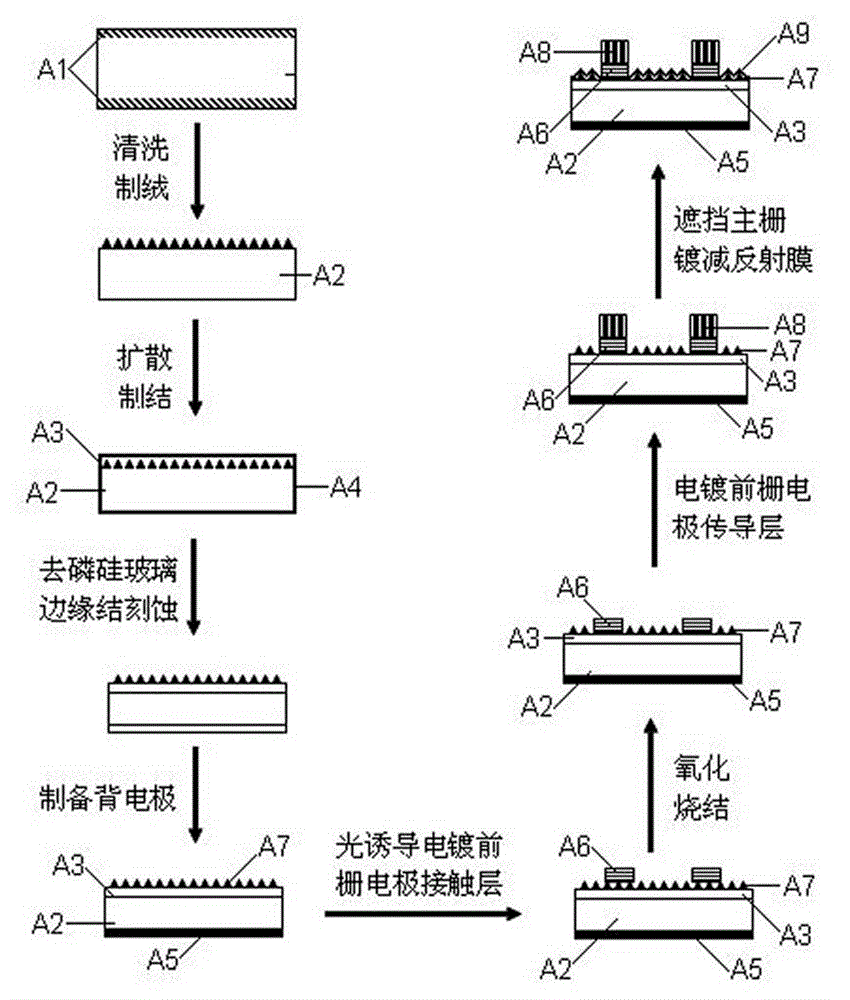
[0037] The prepared 0.01mol / L Co metal ion (CoSO 4 ) The light-induced electroplating electrolyte is injected into the electrolytic cell, and the silicon wafer with the back electrode after texturing, diffusion, etching, dephosphorization, and the back electrode is electrically connected to the electrolytic cell and its control circuit, that is, the back electrode of the silicon wafer and the The Cu counter electrode and the power circuit are well connected, the position of the silicon wafer is fixed and the surface of the N area is kept parallel to the electrolyte surface, and the surface of the N area of ​​the silicon wafer is immersed in the electrolyte. A grid-shaped shading plate is set between the surface of the N-zone of the battery silicon wafer and the fluorescent light source and ensured that it is parallel to the surface of the N-zone, and the light source is activated so that the light passes through the grid-shaped shading plate and irradiates the surface of the N-...

Embodiment 2

[0039] With 1mol / L Ni metal ion (NiSO 4 ) Electrolyte as light-induced electroplating solution, with Cu electrode as counter electrode, Ag as deposited metal, natural light as light source, prepare the front gate electrode of silicon wafer according to the same process steps as in Example 1, and then place the silicon wafer in oxygen Oxidize and sinter at 780°C for 20 minutes in a nitrogen mixed atmosphere (oxygen flow rate 6L / min, nitrogen flow rate 10L / min), then electroplate a metal Sn conductive layer on the contact layer, and prepare a layer on the surface of the solar cell substrate by physical sputtering TiO 2 The anti-reflection film is processed to obtain the original plate of the crystalline silicon solar cell. After testing, the series resistance is lower than that of batteries prepared in the prior art.

Embodiment 3

[0041] With 0.3mol / L Co metal ion (CoSO 4 ) Electrolyte as light-induced electroplating solution, with Cu electrode as counter electrode, Sn as deposited metal, with LED lamp as light source, prepare the front grid electrode of silicon wafer according to the same process steps as in Example 1, and then place the silicon wafer in Oxidize and sinter at 780°C for 20 minutes in a pure oxygen atmosphere (flow rate 6L / min), then electroplate a metal Ag conductive layer on the contact layer, and prepare a layer of Si on the surface of the solar cell substrate by gel sol method 3 N 4 The anti-reflection film is processed to obtain the original plate of the crystalline silicon solar cell. After testing, the series resistance is lower than that of batteries prepared in the prior art.


PUM


Abstract

The invention discloses a crystalline silicon solar cell with high-photoelectric conversion efficiency and a manufacturing method thereof. The cell comprises a crystalline silicon P-N node substrate, a back electrode and a front gate electrode, wherein the back electrode is in ohmic contact with the P area of the crystalline silicon P-N node substrate; the front gate electrode is in ohmic contact with the N area of the crystalline silicon P-N node substrate; the front gate electrode is wrapped under the antireflection layer and comprises a SiO2 layer and an antireflection layer; the SiO2 layer is positioned on the surface of the N area of the crystalline silicon P-N node substrate; and the antireflection layer is arranged on the SiO2 layer. The manufacturing method comprises a cleaning and flocking step, a diffusing and knotting step, a phosphorus-washing and etching step, a back electrode-preparing step, a photoinduced front gate electrode electroplating step, an oxidizing and sintering step, a front gate electrode electroplating step and an antireflection layer preparing step. The photoinduced front gate electrode electroplating step and the oxidizing and sintering step are adopted, so that the cell has the characteristics of simple production process, high efficiency, low cost, low front gate electrode shade loss of the solar cell, low contact resistance and body resistance, uneasiness in line breaking of the thin front gate electrode, low cell surface reflectivity and high photoelectric conversion efficiency.

Description

technical field [0001] The invention belongs to the technical field of solar energy utilization, and in particular relates to a crystalline silicon solar cell with a high photoelectric conversion rate and a manufacturing method thereof. Background technique [0002] When non-renewable energy sources such as electricity, coal, and oil are running out frequently, and energy issues have increasingly become a bottleneck restricting the development of the international society and economy, more and more countries have begun to implement the "Sunshine Plan" to develop solar energy resources and seek new impetus for economic development. Solar photovoltaic power generation will occupy an important seat in the world's energy consumption in the near future, not only to replace some conventional energy sources, but also to become the main body of the world's energy supply. It is estimated that by 2030, renewable energy will account for more than 30% of the total energy structure, and ...

Claims


Application Information

Patent Timeline
Patent Type & Authority Applications(China)
IPC IPC(8): H01L31/0224H01L31/0216H01L31/18
CPCY02P70/50
Inventor 刘铸肖辉徐哲冯苑飞
Owner YUNNAN UNIV
Why Eureka
Try Eureka