A high-resolution biosensor

A biosensor, high-resolution technology, applied in the field of sensors, can solve the problems of complex device structure, and achieve the effects of simple preparation method, firm structure, and avoiding pollution

Active Publication Date: 2016-12-14
ZHEJIANG UNIV
View PDF6 Cites 0 Cited by
  • Summary
  • Abstract
  • Description
  • Claims
  • Application Information

AI Technical Summary

Problems solved by technology

However, nanopore technology still faces many challenges: For example, it is difficult to prepare pores with a diameter of less than 2 nm with current technology. How to reduce the speed at which DNA passes through nanopores? How to control the structural morphology of DNA as it passes through the nanopore? How to integrate atomic-scale electrodes into nanopores to achieve single-base resolution? In order to solve the technical problems faced, the invention patent (publication number: JP2011-45944; application number: 201110097791.0) proposed by the applicant of this patent proposes the use of conductive layered materials such as graphene with an atomic layer thickness to achieve the resolution of a single base rate, and the structure of micro-nanofluidic devices is used to control the movement of DNA molecules; however, the structures of these devices are relatively complex

Method used


Image

  • A high-resolution biosensor
  • A high-resolution biosensor
  • A high-resolution biosensor

Examples


Embodiment 1

[0035]Embodiment 1: synthesis and transfer graphene film

[0036] Graphene film was synthesized on Cu by chemical vapor deposition method: the surface of Cu sheet with a thickness of 25 μm was polished and cleaned, and it was placed in an ultra-high vacuum (1×10 -8 torr), then in Ar / H 2 In atmosphere (~20 vol% H 2 ) for about 110 minutes at 750 ºC, then raise the temperature to ~950 ºC for 30 minutes; turn off the Ar / H 2 , while the modified CH 4 To synthesize the graphene film, the growth time is 5 minutes, thus the graphene film is synthesized.

[0037] After the graphene film is synthesized, spin-coat 500 nm Polymethylmethacrylate (PMMA) layer on the synthesized graphene film, the graphene film / Cu that will be coated with PMMA is placed in ferric nitrate solution and Cu is corroded, PMMA / graphene The film was separated from the Cu substrate, resulting in a PMMA / graphene film. Then, the PMMA / graphene film was transferred to the Al 2 o 3 (100 nm) / Si(550 µm) in Al 2 ...

Embodiment 2

[0038] Embodiment 2: Graphene is as the biosensor of sensitive functional layer

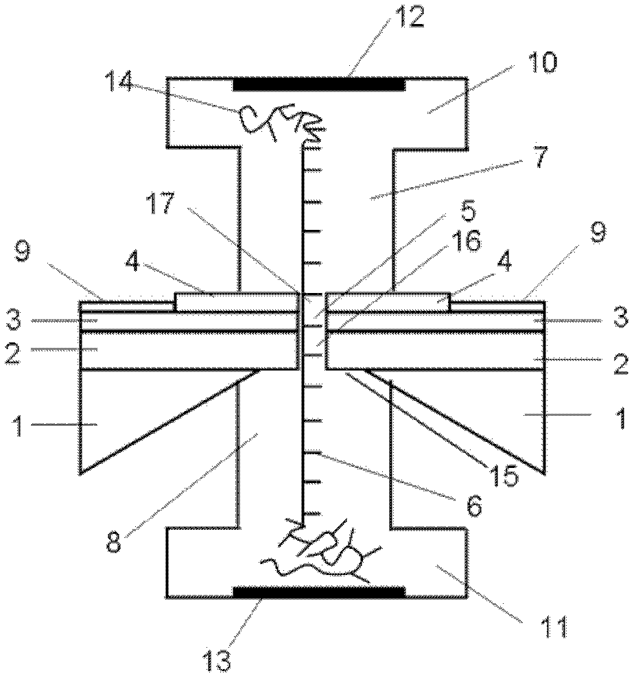
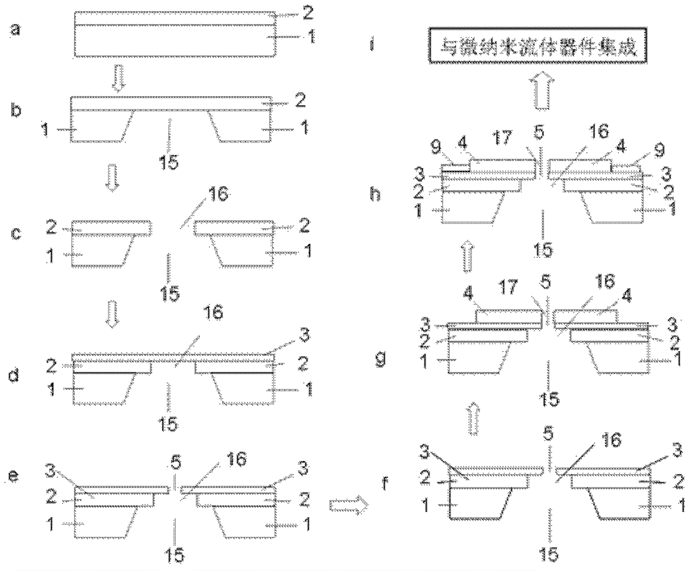
[0039] Such as figure 2 Shown: 100 nm Al prepared on a 550 µm thick Si substrate1 2 o 3 The first insulating layer 2 ( figure 2 a).

[0040] Using photolithography and mask technology, and etching the silicon substrate with KOH solution to prepare a square opening 15 ( figure 2 b).

[0041] Using photolithography and mask technology, and using buffered HF solution to etch the Al on the square opening of the silicon substrate 2 o 3 Thus a hole 16 with a diameter of 10 mm ( figure 2 c).

[0042] Transfer the prepared graphene film to Al 2 o 3 (100 nm) / Si(550 µm) in Al 2 o 3 As the sensitive functional layer 3 on the first insulating layer, the graphene film covers Al 2 o 3 hole 16 ( image 3 ).

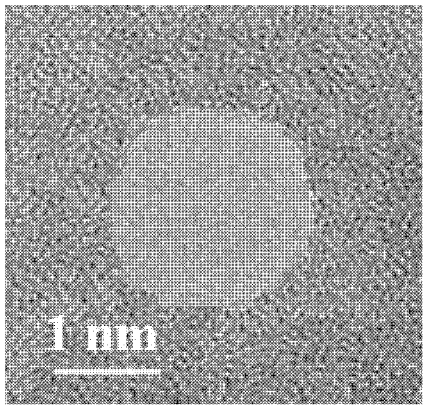
[0043] Fabrication of graphene nanopores using an electron beam from a transmission electron microscope (JEOL 2010F) 5: Adjust the magnification of the transmission electron microscope...

Embodiment 3

[0048] Example 3: MoS 2 Biosensors as sensitive functional layers

[0049] Such as Figure 4 Shown: 50 nm SiO fabricated sequentially on a 600 µm thick monocrystalline Si substrate 1 2 and 30 nm Si 3 N 4 Composite insulating layer 2 ( Figure 4 a).

[0050] Using photolithography technology, and using KOH solution and buffered HF solution to etch the silicon substrate and SiO 2 And prepare a square opening 15 ( Figure 4 b).

[0051] E-beam etching with SF 6 Plasma Reactive Etching Technology in Si 3 N 4 A hole 16 ( Figure 4 c).

[0052] Bilayer MoS produced by mechanical exfoliation 2 Thin films transferred to Si 3 N 4 (30nm) / SiO 2 (50 nm) / Si of Si 3 N 4 As a sub-nanometer functional layer3, MoS 2 Thin film covered silicon nitride membrane holes 16 ( Figure 4 d).

[0053] Preparation of MoS using electron beam from transmission electron microscopy (JEOL 2010F) 2 Nanopore 5: Adjust the magnification of the transmission electron microscope to about 800...


PUM

PropertyMeasurementUnit
thicknessaaaaaaaaaa
thicknessaaaaaaaaaa
thicknessaaaaaaaaaa

Abstract

The invention discloses a high-resolution biosensor, which includes an atomic-scale conductive material as a sensitive unit to achieve atomic-level detection resolution and a micro-nano fluid device to control the motion and morphological structure of detected molecules. The second electrophoretic electrode or micropump, the second storage room, the second micro-nano separation channel, the substrate, the first insulating layer, the sensitive functional layer, the second insulating layer, the first micro-nano separation channel, the first storage room, the first The electrophoretic electrodes or micropumps are placed in sequence, the center of the sensitive functional layer is provided with nanopores, the center of the first insulating layer is provided with openings in the first insulating layer, the center of the second insulating layer is provided with openings in the second insulating layer, and the substrate A substrate opening is arranged in the center of the substrate, and an electrical contact layer for measuring electrical signals is arranged on the sensitive functional layer. The sensitive functional layer with an atomic layer thickness of the present invention enables the resolution of the sensor to reach the atomic scale, and the integration with the micro-nano fluidic device can control the movement and structure of DNA or RNA, so that stable signal detection can be obtained.

Description

technical field [0001] The invention relates to a sensor, in particular to a high-resolution biosensor. Background technique [0002] Gene electronic sequencing has the advantages of high accuracy, low cost, and high speed. Nanopore is currently the most researched single-molecule electronic sequencing technology. Nanopores are expected to be able to detect and characterize biomolecules such as DNA, RNA, and peptides at the single-molecule resolution level. Potential nanopore-based single-molecule gene sequencing technology does not require fluorescent markers or PCR reactions, and is expected to be able to directly and quickly " Read" the base sequence of DNA or RNA; this sequencing technology is expected to greatly reduce the cost of sequencing and realize personalized medicine. However, nanopore technology still faces many challenges: For example, it is difficult to prepare pores with a diameter less than 2 nm in current technology. How to reduce the speed at which DNA p...

Claims


Application Information

Patent Timeline
Patent Type & Authority Patents(China)
IPC IPC(8): C12M1/34
Inventor 徐明生陈红征吴刚施敏敏汪茫
Owner ZHEJIANG UNIV
Why Eureka
Try Eureka