

Preparation method for three-dimensional metal micro-nanometer device
A micro-nano, metal technology, applied in the field of manufacturing micro-nano devices, can solve the problems of inability to flexibly design metal structures, limit the diversity of metal structures, limit the scope of application, etc., and achieve the effect of improving strength, low cost, and expanding functions
- Summary
- Abstract
- Description
- Claims
- Application Information
AI Technical Summary
Problems solved by technology
Method used
Image

Examples
Embodiment 1
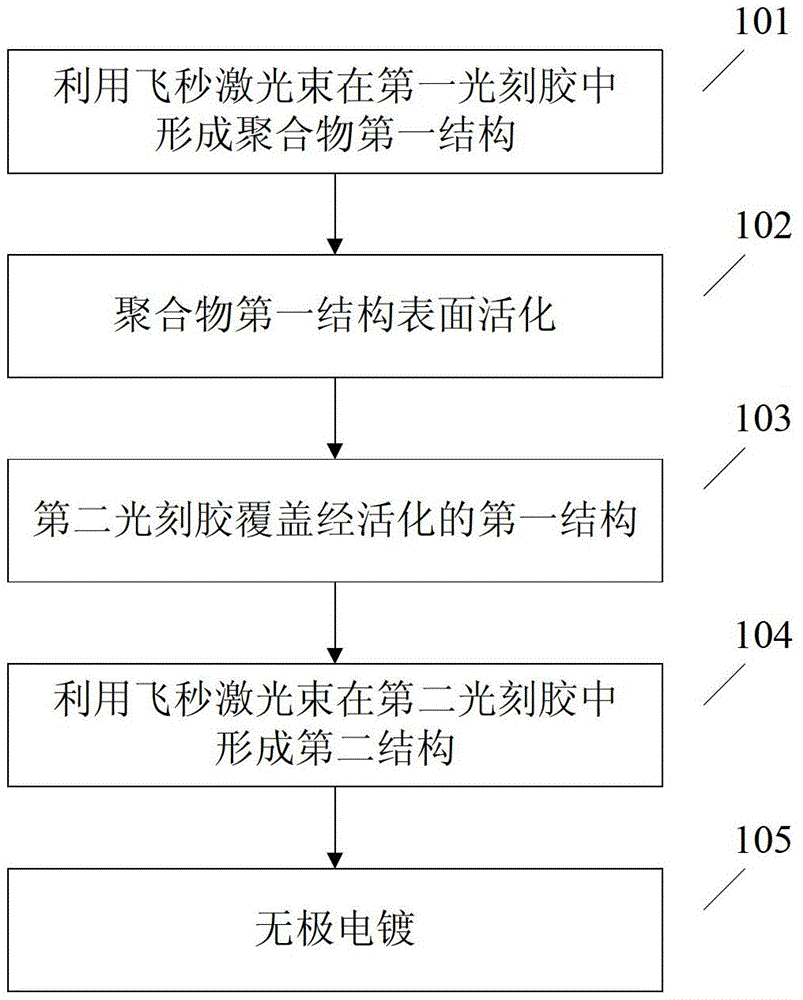
[0057] The method for preparing a three-dimensional metal submicron inductor by using the step-by-step laser direct writing technology and the electrodeless electroplating process comprises the following steps:
[0058] 1) Using femtosecond laser direct writing technology to process the polymer scaffold structure, that is, the first structure.
[0059] Using the femtosecond laser processing system shown in Figure 3 in the document "Femtosecond pulsed laser two-photon micro-nano processing technology and its application, Science Bulletin, 2008, Volume 53, Issue 1, 2-13", the laser light source is selected for mode-locking The titanium-sapphire laser has a central wavelength of 780nm, a pulse width of 80fs, and a repetition rate of 80MHz. A shutter and an attenuator are placed in the optical path to adjust the exposure time and light intensity of the laser, and a 100x oil-immersion objective lens with a numerical aperture of 1.42 is used for focusing.
[0060] A negative photor...
Embodiment 2
[0075] The method for making wires according to the present invention will be described in detail below with reference to the accompanying drawings, including the following steps:
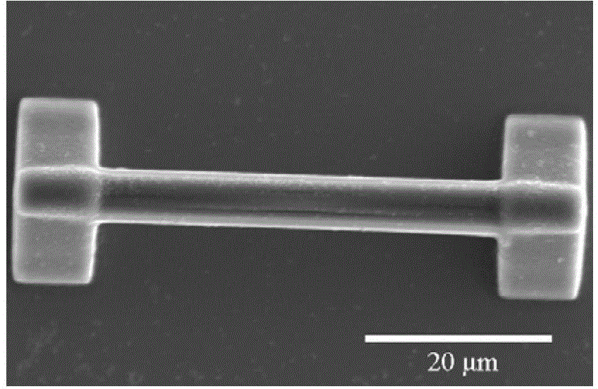
[0076] 1) Using femtosecond laser direct writing technology to form the first wire structure
[0077] Drop the negative photoresist SCR500 on the glass substrate. Use the femtosecond laser processing system and method described in Step 1) of Example 1 to scan and expose a cuboid structure with a length, width and height of 70 μm, 2 μm and 3.5 μm, respectively, as the first wire structure. The height stated herein is the distance of the resulting structure from the surface of the substrate. The exposed sample is placed in ethanol for development, and the unexposed part is washed away to obtain the polymer first wire structure.
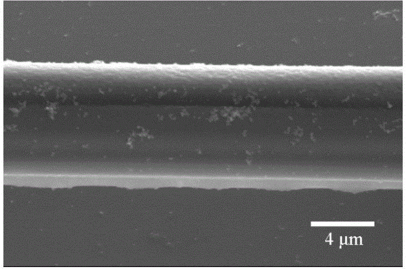
[0078] 2) Surface activation of polymer structures
[0079] 0.5gSnCl 2Dissolve in the solution obtained by mixing 28ml of water and 2ml of hydrochloric acid to obtain an...
Embodiment 3
[0086] A method for manufacturing a resistor with lead wires by using step-by-step laser direct writing technology and an electrodeless plating process, comprising the following steps:
[0087] 1) Using femtosecond laser direct writing technology to process the first wire structure.
[0088] Drop the negative photoresist SCR500 on the glass substrate. Use the femtosecond laser processing system and method described in step 1) of Example 1 to scan and expose a cuboid structure with a length, width and height of 70 μm, 2 μm and 3.5 μm respectively as a wire structure, and place the exposed sample in ethanol for development , to wash away the unexposed parts to obtain the first structure of the polymer.
[0089] 2) Surface activation of polymer structures
[0090] 0.5gSnCl 2 Dissolve in the solution obtained by mixing 28ml of water and 2ml of hydrochloric acid to obtain an aqueous solution of divalent tin salt. The wire structure is soaked in the divalent tin salt aqueous sol...
PUM
| Property | Measurement | Unit |
|---|---|---|
| wavelength | aaaaa | aaaaa |
| thickness | aaaaa | aaaaa |
| electrical resistance | aaaaa | aaaaa |
Abstract
Description
Claims
Application Information