Preparation method of matrix surface nano compound Me-Si-N superhard coating
A nano-composite, me-si-n technology, applied in the field of preparation of nano-composite Me-Si-N superhard coating on the surface of the substrate, can solve the problems of rough film surface, low film hardness and low metal ionization rate
- Summary
- Abstract
- Description
- Claims
- Application Information
AI Technical Summary
Problems solved by technology
Method used
Image
Examples
Embodiment 1
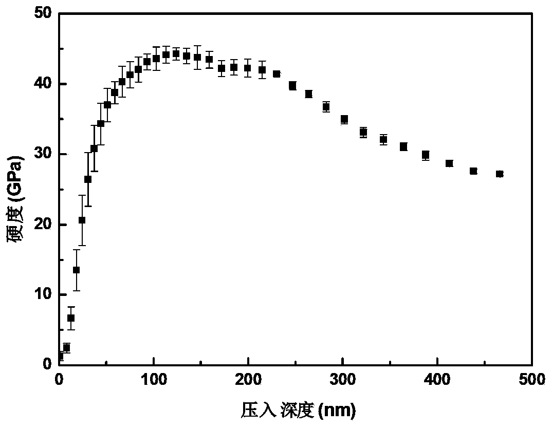
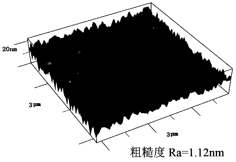
[0032] In this embodiment, the high-speed steel is used as the substrate, and the TiSiN nanocomposite coating is deposited on the surface of the substrate by using high-power pulsed magnetron sputtering technology. The specific preparation process is as follows.
[0033] (1) Put the cleaned and dried substrate into the vacuum chamber until the air pressure in the chamber is 3×10 -3 At Pa, argon gas was introduced into the vacuum chamber so that the chamber pressure was 8.0mTorr, the substrate pulse negative bias was -400V, and the substrate was etched for 20 minutes by glow discharge;
[0034] (2) After the etching is completed, Ar is introduced into the cavity, so that the cavity pressure is 2mTorr, the high-power pulse magnetron sputtering source is turned on, and the alloy target TiSi target is deposited by high-power pulse magnetron sputtering to deposit the TiSi transition layer , the substrate negative bias voltage is -300V, the sputtering DC current is 2A, the pulse con...
Embodiment 2
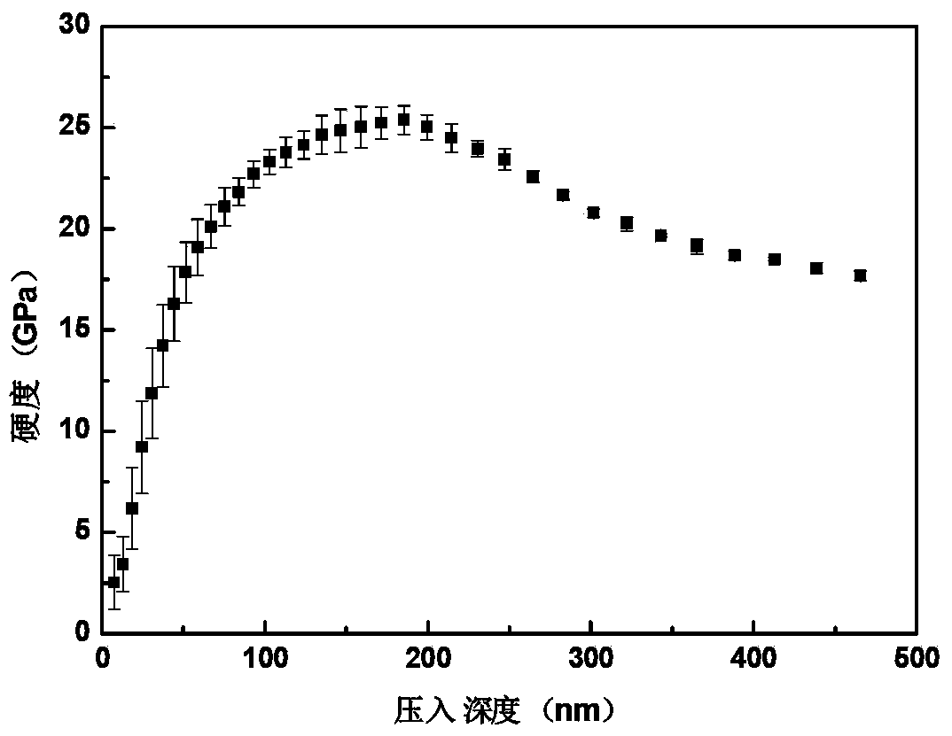
[0040] In this embodiment, the substrate is exactly the same as that in Embodiment 1, and a TiSiN nanocomposite coating is deposited on the surface of the substrate by high-power pulse magnetron sputtering technology, and the specific preparation process is as follows.
[0041] (1) Exactly the same as step (1) in Example 1;
[0042] (2) It is basically the same as step (2) in Example 1, the difference is: when using the high-power pulse magnetron sputtering alloy target TiSi target to deposit the TiSi transition layer, the negative bias of the substrate is -300V, and the sputtering The DC current is 1A, the pulse constant voltage is 450V, the pulse frequency is 40Hz, and the pulse width is 80 microseconds;
[0043] (3) It is basically the same as step (2) in Example 1, the difference is: use high-power pulse magnetron sputtering alloy target TiSi target to deposit TiSiN nanocomposite coating; substrate negative bias is -100V, sputtering The pulse constant current is 1A, the p...
Embodiment 3
[0048] In this embodiment, the high-speed steel is used as the substrate, and the CrSiN nano-composite coating is deposited on the surface of the substrate by high-power pulsed magnetron sputtering technology, and the specific process is as follows.
[0049] (1) Put the cleaned and dried substrate into the vacuum chamber until the air pressure in the chamber is 3×10 -3 At Pa, argon gas was introduced into the vacuum chamber so that the chamber pressure was 8.0mtorr, the substrate pulse negative bias was -400V, and the substrate was etched for 20 minutes by glow discharge;
[0050] (2) After the etching is completed, Ar is introduced into the cavity, so that the cavity pressure is 2mTorr, the high-power pulse magnetron sputtering source is turned on, and the CrSi transition layer is deposited by using the high-power pulse magnetron sputtering metal target CrSi target, The substrate negative bias is -300V, the sputtering pulse constant current is 2A, the pulse constant voltage i...
PUM
| Property | Measurement | Unit |
|---|---|---|
| Surface roughness | aaaaa | aaaaa |
| Hardness | aaaaa | aaaaa |
Abstract
Description
Claims
Application Information


