Laterally diffused metal-oxide-semiconductor transistor and manufacturing method thereof

A technology of oxide semiconductors and transistors, applied in semiconductor/solid-state device manufacturing, semiconductor devices, electrical components, etc., can solve problems such as unstable device performance, increased cost, and increased photolithography processes

Active Publication Date: 2016-08-03
WILL SEMICON (SHANGHAI) CO LTD
View PDF10 Cites 0 Cited by
  • Summary
  • Abstract
  • Description
  • Claims
  • Application Information

AI Technical Summary

Problems solved by technology

[0012] The technical problem to be solved by the present invention is to overcome the defects in the prior art that the source, drain and gate are drawn out from the front of the wafer, the area of ​​the gate electrode is limited in design so that the on-resistance cannot be reduced, and in order to reduce the conduction The source resistance increases due to the on-resistance and the device performance is unstable, and the photolithography process is added to reduce the on-resistance, which increases the cost and causes the source resistance to increase and the device performance is unstable. Provide a A LDMOS fabrication method that reduces the on-resistance without increasing the photolithography process, and at the same time does not increase the source resistance and drain-source voltage, and is perfectly compatible with the existing CMOS process, and the LDMOS

Method used


Image

  • Laterally diffused metal-oxide-semiconductor transistor and manufacturing method thereof
  • Laterally diffused metal-oxide-semiconductor transistor and manufacturing method thereof
  • Laterally diffused metal-oxide-semiconductor transistor and manufacturing method thereof

Examples


Embodiment 1

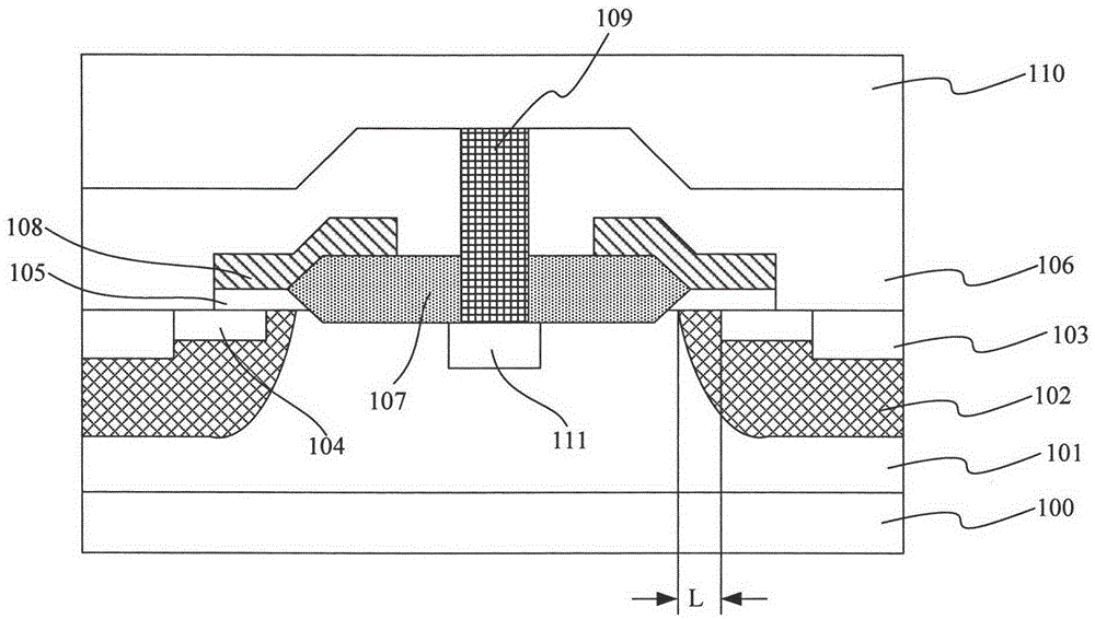
[0112] refer to Figure 4First, an N-type epitaxial layer 201 is formed on the surface of a P-type substrate 200 through an epitaxial process. Wherein, the P-type substrate 200 is a high-concentration doped raw silicon wafer, the resistivity of the P-type substrate is 0.001ohm·cm, the N-type epitaxial layer 201 is formed by an epitaxial process, and the N-type epitaxial layer 201 is used as the drain of the LDMOS, which will withstand a relatively high source-drain voltage. In this embodiment, the resistivity of the N-type epitaxial layer is 0.3 ohm·cm, and the thickness is 3 μm. The specific epitaxial growth process conditions are as follows: silane pyrolysis method is used for vapor phase epitaxy, the reactant is silane, N-type dopant phosphine, the epitaxy temperature is 1100° C., and the time is 20 minutes. The epitaxial thickness is determined according to the LDMOS operating voltage, that is, the source-drain voltage. The higher the voltage, the higher the thickness.

...

Embodiment 2

[0138] The principle of embodiment 2 is the same as embodiment 1, and its main steps are also the same, and the difference only lies in the selection of the following process parameters:

[0139] The resistivity of the P-type substrate is 0.01 ohm·cm, the resistivity of the N-type epitaxial layer is 1.0 ohm·cm, and the thickness is 5 μm, and the epitaxy temperature for forming the N-type epitaxial layer is 1200° C. for 40 minutes.

[0140] First grown by thermal oxidation process thickness of The lining oxide layer, and then deposit silicon nitride by low-pressure chemical vapor deposition process, wherein the thickness of silicon nitride is The thickness of the field oxide layer 207 grown by the thermal oxidation process is

[0141] The formation condition of the P-type doped region 202 is: the dopant dose is 1e14cm -2 The boron ions are accelerated to 200keV for P-type ion implantation to form a P-type doped region 202 in the N-type epitaxial layer.

[0142] The ion i...

Embodiment 3

[0154] The principle of embodiment 3 is the same as embodiment 1, and its main steps are also the same, and the difference only lies in the selection of the following process parameters:

[0155] The resistivity of the P-type substrate is 0.005 ohm·cm, the resistivity of the N-type epitaxial layer is 0.8 ohm·cm, and the thickness is 7 μm, and the epitaxy temperature for forming the N-type epitaxial layer is 1150° C. for 45 minutes.

[0156] The formation condition of the P-type doped region 202 is: the dopant dose is 5e14cm -2 The boron ions are accelerated to 150keV for P-type ion implantation to form a P-type doped region 202 in the N-type epitaxial layer.

[0157] The ion implantation conditions of arsenic ions are: energy: 50keV; doping dose: 5e16cm -2 .

[0158] The thermal driving conditions for forming the P well are: the thermal driving temperature is 1050° C., the thermal driving time is 100 minutes, and the channel length L is 1.5 μm.

[0159] The thickness of the...


PUM


Abstract

The invention discloses an LDMOS which comprises a P-type substrate, an N-type epitaxial layer, a P trap, a first N-type doping region, a groove, a first metal layer and a source-electrode metal layer. The P trap is located in the N-type doping region, the first N-type doping region is arranged in the P trap, and the groove penetrates through the first N-type doping region, the P trap and the N-type epitaxial layer until the P-type substrate. A first oxidation layer is arranged on the side wall of the groove. The groove is filled with first polycrystalline silicon of P-type doping. The upper surface of the first polycrystalline silicon is located inside the P trap and is lower than the first N-type doping region. The first metal layer covers the upper surface of the first polycrystalline silicon and covers the first N-type doping region. The source-electrode metal layer is located on the back face of the P-type substrate. The invention further discloses a manufacturing method of the LDMOS. A source electrode is led out from the back face of the substrate instead of being originally led out from the front face of the substrate, the design area of the original source electrode region on the front face is effectively reduced, the design width of a channel in a gate region is increased, and the on resistance is reduced.

Description

technical field [0001] The invention relates to an LDMOS and a manufacturing method thereof, in particular to an LDMOS and a manufacturing method thereof in which the source electrode is led out from the back of the wafer and is perfectly compatible with the existing CMOS technology. Background technique [0002] LDMOS (LateralDoubleDiffusedMetalOxideSemiconductor, laterally diffused metal oxide semiconductor transistor) has a fast switching speed, can meet high breakdown voltage applications, can withstand higher power than bipolar transistors, has a higher operating frequency, and is easier to integrate with Bi-CMOS (BipolarComplementaryMetalOxideSemiconductor, bipolar and complementary metal oxide semiconductor) integrated circuit technology is compatible and can form a BCD (BipolarCMOSDMOS, double CMOS integrated circuit technology) circuit as its high-voltage unit and other advantages and is widely used. DCMOS circuits are widely used in drivers, High frequency power am...

Claims


Application Information

Patent Timeline
Patent Type & Authority Patents(China)
IPC IPC(8): H01L29/78H01L29/417H01L21/336
Inventor 纪刚顾建平
Owner WILL SEMICON (SHANGHAI) CO LTD
Why Eureka
Try Eureka