Gas-assisted organic field-effect transistor sensor, and preparation method and applications thereof
A transistor and sensor technology, applied in the field of gas-assisted field effect transistor sensor and its preparation, can solve the problems of increased complexity and achieve the effects of wide versatility, simple preparation process and low cost
- Summary
- Abstract
- Description
- Claims
- Application Information
AI Technical Summary
Problems solved by technology
Method used
Image

Examples
Embodiment 1
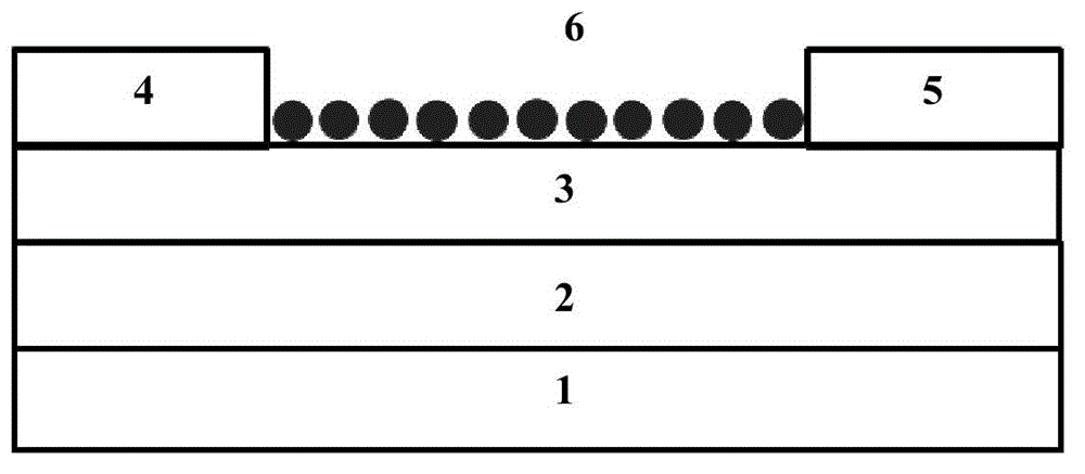
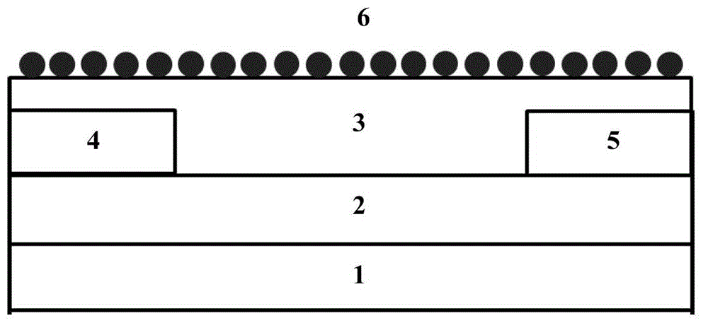
[0066] 1) A phosphorus-doped silicon wafer deposited with a silicon dioxide layer with a thickness of 300nm (the thickness of the silicon wafer layer is 300μm, and the doping mass percentage concentration of phosphorus is 1.5%) is subjected to secondary water, ethanol, and acetone ultrasonic waves. , rinsed, and dried with nitrogen, using H 2 SO 4 :H 2 o 2 = 7:3 (volume ratio) mixed solution soaked for 30min, then ultrasonically cleaned with secondary water, put 1 drop of dodecyltrichlorosilane in a petri dish, dried and placed in a vacuum drying oven for processing A self-assembled monolayer of dodecyltrichlorosilane is formed on the surface of the silicon dioxide layer to obtain an insulating layer;
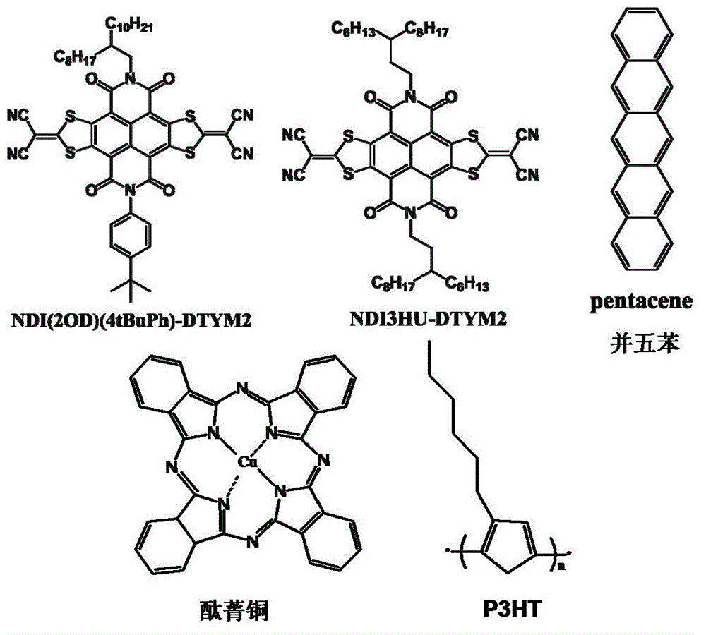
[0067] 2) Spin-coat the naphthalimide derivative NDI(2OD)(4tBuPh)-DTYM2 on the insulating layer obtained in step 1) at a speed of 7000rpm using n-hexane, absolute ethanol, and chloroform for ultrasonication, flushing, and nitrogen blow-drying (see image 3 ), and heat treat...
Embodiment 2
[0080] Embodiment 2, the detection of gas by the organic field effect transistor sensor obtained in embodiment 1
[0081] 1) Detection of HCl gas:
[0082] After the organic field effect transistor sensor obtained in Example 1 was placed in a linear working state and reached a stable state, hydrogen chloride (HCl) gas with a concentration of 10 ppm was introduced.
[0083] The response curve of the source-drain current and time of the device exposed to 10ppm hydrogen chloride gas is as follows Figure 4 It can be seen from the figure that the source-drain current of the device drops and recovers rapidly. It can be seen that based on the above-mentioned organic field effect transistor sensor, using ammonia gas as the receiving layer can realize the effective detection of HCl gas and recover quickly, with a detection limit of 10 ppm.
[0084] Follow the same steps as above, replacing the concentration of hydrogen chloride (HCl) gas with 50, 80, 100, 300ppm.
[0085] The resul...
Embodiment 3
[0094] 1) A phosphorus-doped silicon wafer deposited with a silicon dioxide layer with a thickness of 300nm (the thickness of the silicon wafer layer is 300μm, and the doping mass percentage concentration of phosphorus is 1.5%) is subjected to secondary water, ethanol, and acetone ultrasonic waves. , rinsed, and dried with nitrogen, using H 2 SO 4 :H 2 o 2 = 7:3 (volume ratio) mixed solution soaked for 30min, then ultrasonically cleaned with secondary water, put 1 drop of dodecyltrichlorosilane in a petri dish, dried and placed in a vacuum drying oven for processing A self-assembled monolayer of dodecyltrichlorosilane is formed on the surface of the silicon dioxide layer;
[0095] 2) Use n-hexane, absolute ethanol, chloroform to ultrasonically wash, dry with nitrogen, and then place it in a vacuum coating machine at a vacuum degree of 7×10 -4 Under the condition of Pa The speed of vapor deposition of pentacene (see image 3 ) with a thickness of 20nm to obtain an organic...
PUM
| Property | Measurement | Unit |
|---|---|---|
| Thickness | aaaaa | aaaaa |
| Thickness | aaaaa | aaaaa |
| Thickness | aaaaa | aaaaa |
Abstract
Description
Claims
Application Information
 - Generate Ideas
- Intellectual Property
- Life Sciences
- Materials
- Tech Scout
- Unparalleled Data Quality
- Higher Quality Content
- 60% Fewer Hallucinations
Browse by: Latest US Patents, China's latest patents, Technical Efficacy Thesaurus, Application Domain, Technology Topic, Popular Technical Reports.
© 2025 PatSnap. All rights reserved.Legal|Privacy policy|Modern Slavery Act Transparency Statement|Sitemap|About US| Contact US: help@patsnap.com