Positive and negative photoresist technology combined microstrip line manufacturing method
What is AI technical title?
AI technical title is built by Patsnap AI team. It summarizes the technical point description of the patent document.
A manufacturing method and technology of microstrip lines, which are applied in the manufacture of microstructure devices, metal material coating processes, processes for producing decorative surface effects, etc. Effect
Inactive Publication Date: 2014-01-29
BEIJING INSTITUTE OF TECHNOLOGYGY
View PDF1 Cites 4 Cited by
Summary
Abstract
Description
Claims
Application Information
AI Technical Summary
This helps you quickly interpret patents by identifying the three key elements:
Problems solved by technology
Method used
Benefits of technology
Problems solved by technology
However, in the millimeterwave band, as the frequency increases, the requirements for processing accuracy are getting higher and higher. Traditional machining can no longer meet the requirements, and new processing technologies must be used, and MEMS micro-processing technology can meet the requirements of processing accuracy.
Method used
Image
Click on the blue label to locate the original text in one second.
Reading with bidirectional positioning of images and text.
Examples
Embodiment 1
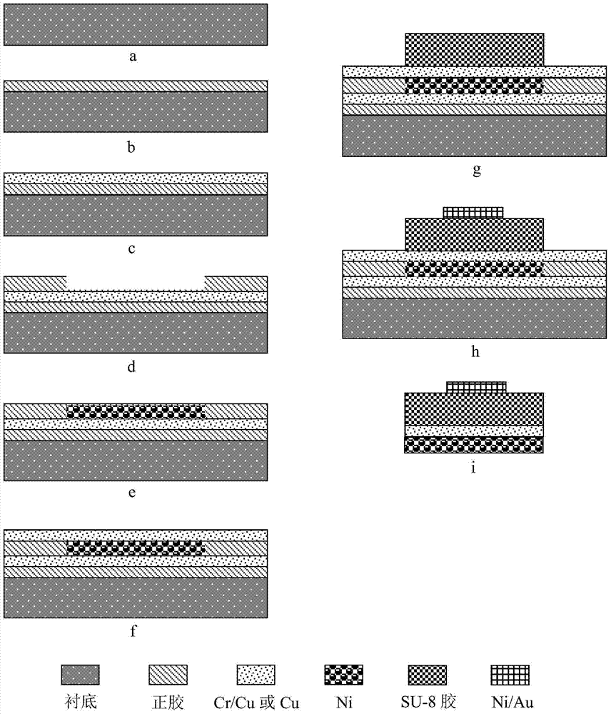
[0022] A microstrip line manufacturing method combining positive and negative glue technology, comprising the following steps:
[0023] (1) Put a certain size of glass or siliconwafer (such as 4 inches) 2 SO 4 +H 2 o 2 , deionized water in order to wash, dry, and then evaporate HMDS (a coupling agent) on the substrate.
[0024] (2) Coat AZ4620 positive photoresist on the treated substrate with a thickness of 5 μm by spin coating.
[0025] (3) Pre-baking the photoresist on a hot plate, the conditions are 65°C / 30min, 95°C / 60min, 120°C / 60min, and cool with the furnace.
[0026] (4) Deposit Cr / Cu seed layer with magnetron multi-target sputtering machine,
[0027] (5) Coating AZ4620 positive resist, 10 μm, on the Cr / Cu seed layer.
[0028] (6) Pre-bake the photoresist on a hot plate, the conditions are 65°C / 30min, 95°C / 60min, and cool with the furnace.
[0046] (1) Wash a glass or silicon wafer of a certain size (such as 4 inches) with H2SO4+H2O2 and deionized water in sequence, dry it, and then evaporate HMDS (a coupling agent) on the substrate.
[0047] (2) Coat the ARP positive photoresist on the processed substrate by spin coating, with a thickness of 10 μm.
[0048] (3) Pre-bake the photoresist with a program-controlled oven, the conditions are 65°C / 40min, 95°C / 90min, 120°C / 90min, and cool with the furnace.
[0049] (4) Deposit Cu seed layer with magnetron multi-target sputtering machine, thickness
[0050] (5) Coating AZ4620 positive resist, 10 μm, on the Cu seed layer.
[0051] (6) Pre-baking the photoresist with a program-controlled oven, the conditions are 65°C / 400min, 95°C / 90min, and cool with the furnace.
[0054] (9) After the electroplating is completed, the film is hardened, and the condition is 120°C / 6...
PUM
Abstract
The invention discloses a positive and negative photoresist technology combined microstrip line manufacturing method. The positive and negative photoresist technology combined microstrip line manufacturing method includes: 1), spinning a layer of positive photoresist on glass sheets or silicon slices as a device releasing sacrificial layer; 2), deposing a layer of Cu metal on the positive photoresist via the magnetron sputtering technology as an electroplating seed layer; 3), coating the positive photoresist on the Cu seed layer and photoetching; 4), using electroplate Ni as a microstrip line ground layer; 5), sputtering the Cu metal layer; 6), coating SU-8 photoresist on the Cu layer and photoetching; 7), sputtering a Cr / Cu electroplating seed layer; 8), coating photoresist on the SU-8 dielectric layer, and photoetching; 9), electroplating microstrip line; 10), dissolving the positive photoresist with solvent, so that microstrip line devices with the SU-8 photoresist as the dielectric layer are released from glass or silicon slices.
Description
technical field [0001] The invention relates to RF MEMS manufacturing technology, in particular to a manufacturing method of a microstrip line. Background technique [0002] With the development of technology, radio technology is developing towards shorter and shorter millimeterwaves and submillimeter waves. Millimeterwaves are between microwave and light, and have the advantages of wide frequency range, high resolution, all-weather work, and easy integration. Therefore, they are widely used in military, communication, security and other fields. However, in the millimeterwave band, as the frequency increases, the requirements for processing accuracy are getting higher and higher. Traditional machining can no longer meet the requirements, and new processing technologies must be used, and MEMS micro-processing technology can meet the requirements of processing accuracy. . It has the advantages of high precision, good controllability, batch manufacturing, and compatibility...
Claims
Application Information
Patent Timeline
Application Date:The date an application was filed.
Publication Date:The date a patent or application was officially published.
First Publication Date:The earliest publication date of a patent with the same application number.
Issue Date:Publication date of the patent grant document.
PCT Entry Date:The Entry date of PCT National Phase.
Estimated Expiry Date:The statutory expiry date of a patent right according to the Patent Law, and it is the longest term of protection that the patent right can achieve without the termination of the patent right due to other reasons(Term extension factor has been taken into account ).
Invalid Date:Actual expiry date is based on effective date or publication date of legal transaction data of invalid patent.

