Preparation method of boron-doped diamond film/carbon film composite electrode material

A boron-doped diamond and composite electrode technology, which is applied in the field of preparation of conductive diamond electrodes, can solve the problems of high signal-to-noise ratio and poor charge storage capacity

Active Publication Date: 2014-04-02
SICHUAN UNIV
View PDF9 Cites 9 Cited by
  • Summary
  • Abstract
  • Description
  • Claims
  • Application Information

AI Technical Summary

Problems solved by technology

[0005] The characteristics of diamond electrodes include high signal-to-noise ratio, excellent response repeatability and resistance to deactivation and electrode contamination caused by

Method used


Image

  • Preparation method of boron-doped diamond film/carbon film composite electrode material
  • Preparation method of boron-doped diamond film/carbon film composite electrode material
  • Preparation method of boron-doped diamond film/carbon film composite electrode material

Examples


Example Embodiment

[0025] Example 1:

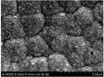
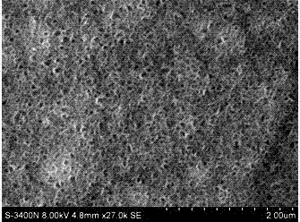
[0026] Deposit a diamond film of more than 5μm on a 2-inch intrinsic silicon wafer. After the surface of the silicon wafer is cleaned by conventional methods, it is ground with diamond powder, and then the wafer is cut into 15×5mm strips and ultrasonically cleaned with ethanol or acetone. 5 After drying for minutes, place it in the antenna bell-type microwave plasma CVD reaction chamber with the silicon surface facing up and the diamond film surface close to the base. The reaction chamber is evacuated and the microwave generator is turned on. The hydrogen bubbling carries the boron trioxide dissolved in acetone (B 2 O 3 ), in CH 4 / H 2 It is 0.5vol%, the B / C ratio is 1 / 100, the working gas pressure is 4.3KPa, and the microwave output power is 1300W for 12 hours. The thickness of the boron-doped diamond film is 5mm, and the square resistance of the four-probe test is 463Ω / □.

Example Embodiment

[0027] Example 2:

[0028] Deposit a diamond film of more than 5μm on a 2-inch intrinsic silicon wafer. After the surface of the silicon wafer is cleaned by conventional methods, it is ground with diamond powder, and then the wafer is cut into 15×5mm strips and ultrasonically cleaned with ethanol or acetone. 5 After drying for minutes, place it in the antenna bell-type microwave plasma CVD reaction chamber with the silicon surface facing up and the diamond film surface close to the base. The reaction chamber is evacuated and the microwave generator is turned on. The hydrogen bubbling carries the boron trioxide dissolved in acetone (B 2 O 3 ), in CH 4 / H 2 It is 0.5vol%, the B / C ratio is 1 / 100, the working gas pressure is 4.3KPa, and the microwave output power is 1300W to extend the deposition time to 20 hours, the thickness of the boron-doped diamond film is 9mm, and the square resistance of the four-probe test is 261Ω / □, the conductivity is enhanced.

Example Embodiment

[0029] Example 3:

[0030] Deposit a diamond film of more than 5μm on a 2-inch intrinsic silicon wafer. After the surface of the silicon wafer is cleaned by conventional methods, it is ground with diamond powder, and then the wafer is cut into 15×5mm strips and ultrasonically cleaned with ethanol or acetone. 5 After drying for minutes, place it in the antenna bell-type microwave plasma CVD reaction chamber with the silicon surface facing up and the diamond film surface close to the base. The reaction chamber is evacuated and the microwave generator is turned on. The hydrogen bubbling carries the boron trioxide dissolved in acetone (B 2 O 3 ), in CH 4 / H 2 Deposition is 0.5vol%, working gas pressure 4.3KPa, microwave output power of 1300W for 12 hours, B / C ratio is 1 / 200, boron-doped diamond film thickness is 5mm, square resistance measured by four probes is 1464Ω / □, Decrease in conductivity.


PUM

PropertyMeasurementUnit
Thicknessaaaaaaaaaa
Square resistanceaaaaaaaaaa
Thicknessaaaaaaaaaa

Abstract

The invention discloses a preparation method of a boron-doped diamond film/carbon film composite electrode material, which is characterized by adopting a conventional diamond film preparation method and comprising the following steps: preparing an insulated diamond film (3) on a non-conductive substrate (2); and preparing a boron-doped diamond film (1) on the other side of the substrate, and partially converting the insulated diamond film into a carbon film (4). Primarily in the preparation of the carbon film, the diamond of the insulated diamond film is partially converted into a non-diamond phase such as graphite and amorphous state carbon under the effect of high temperature and oxygen in a boron source; and the preparation of the carbon film and the preparation of the boron-doped diamond film are performed at the same time. When the composite plane electrode material is in use, electrical stimulation is realized by use of the advantages of low impedance and higher charge storage capacity of the carbon film; and meanwhile, the high signal-to-noise ratio of the boron-doped diamond film is more favorable for detecting electrical signals. Compared with a common electrode preparation method, two electrode materials are prepared on the substrate, and two functions can be realized.

Description

technical field [0001] The invention relates to the preparation of a conductive diamond electrode, specifically a method for preparing a conductive boron-doped diamond film on one side of a non-conductive material surface, and simultaneously preparing a conductive carbon film on the other side to obtain a composite electrode material. technical background [0002] The nervous system is a complex system. Human beings have been trying to explore its mysteries for a long time, so neural engineering is derived, which is an interdisciplinary subject of neuroscience, material science, microelectronics technology and information science. The study of neural engineering systems is of great significance for revealing the working mechanism of the nervous system and exploring the treatment and rehabilitation of neurological diseases. The most critical thing in the neural engineering system is the nerve-electronic interface, that is, the electrode, which mainly realizes the following tw...

Claims


Application Information

Patent Timeline
IPC IPC(8): C23C16/22C23C16/511A61N1/05
Inventor 芶立练发东
Owner SICHUAN UNIV
Why Eureka
Try Eureka