Capacitance Si-based radiation detecting device, and preparation method thereof

A radiation detector and radiation detection technology, applied in the field of microelectronics, can solve the problems of single event effect isolation, low sensitivity response, lack of protection devices, etc., and achieve the effects of reducing the working grid voltage, improving detection accuracy, and improving sensitivity

Active Publication Date: 2014-04-02
NO 771 INST OF NO 9 RES INST CHINA AEROSPACE SCI & TECH
View PDF4 Cites 3 Cited by
  • Summary
  • Abstract
  • Description
  • Claims
  • Application Information

AI Technical Summary

Problems solved by technology

The main problems of this type of RADFET device are as follows: 1) Due to the use of bulk silicon technology, the single event effect is not effectively isolated; 2) In order to suppress the degradation of the threshold voltage of the RADFET device after radiation, generally thicker The gate oxide thickness is too high, which causes the working voltage of the RADFET device to be too high; 3) The existing RADFET devices generally use SiO 2 (SiON) structure gate dielectric, which makes the sensitivity response low; 4) The working time of the existing RADFET device is short, which cannot meet the long-term recording of radiation information data; 5) Lack of protection devices, in the sudden high In a radiation environment, it is easy to cause burnout of MOS dose rate devices

Method used


Image

  • Capacitance Si-based radiation detecting device, and preparation method thereof
  • Capacitance Si-based radiation detecting device, and preparation method thereof
  • Capacitance Si-based radiation detecting device, and preparation method thereof

Examples


Embodiment 1

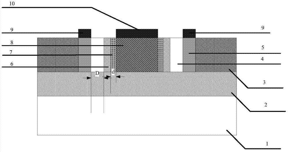
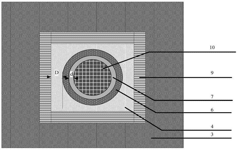
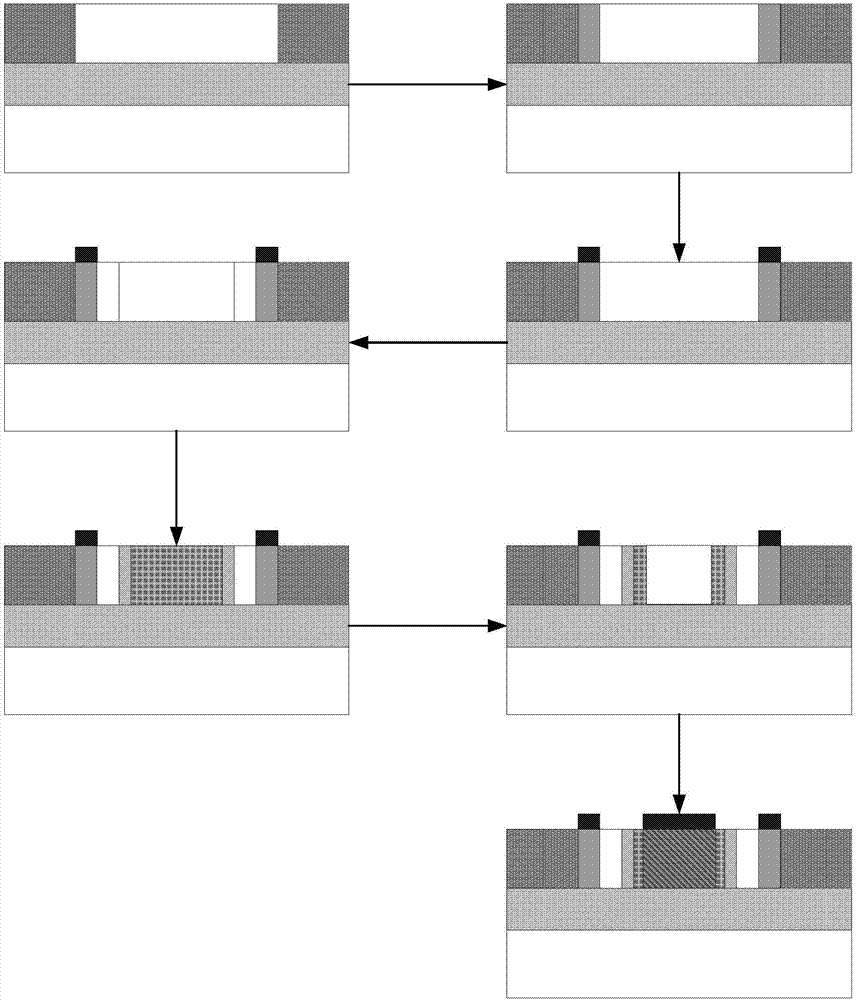
[0044] 1) On the SOI CMOS substrate, use the LOCOS process to grow an oxide isolation layer, wherein the SOI CMOS substrate includes a Si substrate layer and a buried oxide layer above the Si substrate layer.

[0045] The specific steps are: removing all oxide layers on the SOI CMOS substrate, cleaning, and growing SiO with a thickness of 50nm by dry oxygen oxidation. 2 Oxygen pad layer, in which the temperature of the oxidation furnace used is 900°C, the temperature of the oxidation bottle is 85°C, and the oxidation time is 5min; then the Si with a thickness of 220nm is grown by low-pressure chemical vapor deposition (LPCVD). 3 N 4 The masking layer, wherein the deposition pressure is 335Pa, the deposition time is 30min, and the deposition temperature is 850°C; the pattern of the oxide isolation layer is photoetched by photolithography, and the dry oxidation, wet oxidation and dry oxidation are used in sequence The method is to perform high temperature oxidation to obtain an...

Embodiment 2

[0057] 1) On the SOI CMOS substrate, use the LOCOS process to grow an oxide isolation layer, wherein the SOI CMOS substrate includes a Si substrate layer and a buried oxide layer above the Si substrate layer.

[0058] The specific steps are: removing all oxide layers on the SOI CMOS substrate, cleaning, and growing SiO with a thickness of 100nm by dry oxygen oxidation. 2 Oxygen pad layer, in which the temperature of the oxidation furnace used is 950°C, the temperature of the oxidation bottle is 88°C, and the oxidation time is 9min; then the Si with a thickness of 190nm is grown by low-pressure chemical vapor deposition (LPCVD). 3 N 4 Masking layer, wherein the deposition pressure is 32Pa, the deposition time is 55min, and the deposition temperature is 750°C; the pattern of the oxide isolation layer is photoetched by photolithography, and the dry oxidation, wet oxidation and dry oxidation are used in sequence The method is to perform high temperature oxidation to obtain an oxi...

Embodiment 3

[0070] 1) On the SOI CMOS substrate, use the LOCOS process to grow an oxide isolation layer, wherein the SOI CMOS substrate includes a Si substrate layer and a buried oxide layer above the Si substrate layer.

[0071] The specific steps are: remove all oxide layers on the SOI CMOS substrate, clean, and grow SiO with a thickness of 150nm by dry oxygen oxidation. 2 Oxygen pad layer, in which the temperature of the oxidation furnace used is 1000°C, the temperature of the oxidation bottle is 90°C, and the oxidation time is 7 minutes; then the Si with a thickness of 210nm is grown by low-pressure chemical vapor deposition (LPCVD). 3 N 4 Masking layer, wherein the deposition pressure is 29Pa, the deposition time is 50min, and the deposition temperature is 800°C; the pattern of the oxide isolation layer is photoetched by photolithography, and the dry oxidation, wet oxidation and dry oxidation are used in sequence The method is to perform high temperature oxidation to obtain an oxidi...


PUM


Abstract

The invention provides a capacitance Si-based radiation detecting device, and a preparation method thereof. The detecting device comprises an Si substrate layer, wherein a buried oxide layer is set above the Si substrate layer; a metal fill area, a gate dielectric area, a Si thin layer, an ohmic contact injection area and an oxide isolation layer are set on the buried oxide layer from the center to the periphery; an ohmic contact area is set above the ohmic contact injection area; a gate metal electrode is set above the metal fill area. The detector has the advantages of high radiation sensitivity and induced charge capacity, low work gate voltage and high reliability. The method comprises the steps of growing the oxide isolation layer on a substrate; forming the ohmic contact injection area by doping light and heavy ions; forming the ohmic contact area via sputter deposition; forming a groove area via etching; forming the gate dielectric area via an atomic layer deposition process; forming a metal fill groove area via secondary etching; forming the metal fill area and the gate metal electrode via the Cu interconnection process. The method has the advantages of simpleness in process, good repeatability, low cost and easiness in integration with the fabrication process of the existing large-scale integrated circuit.

Description

technical field [0001] The invention belongs to the technical field of microelectronics and relates to semiconductor devices, in particular to a capacitive Si-based radiation detection device and a preparation method thereof. Background technique [0002] Radiation detectors are mainly used to measure various radiation environmental particles, such as photons, neutrons, alpha particles, beta particles and high-energy ions. Therefore, it has a wide range of applications in nuclear physics, medical treatment, biomedical occasions, and aerospace satellite detection and other fields. For example, in the field of space applications, it is necessary to measure the metering rate of particles in the space environment in real time, so as to ensure the normal operation of electronic equipment. [0003] MOS capacitive radiation dosimeter refers to a dosimeter made of semiconductor materials. Under radiation conditions, the gate oxide dielectric region of the device will generate indu...

Claims


Application Information

Patent Timeline
Patent Type & Authority Applications(China)
IPC IPC(8): H01L31/119H01L31/0224H01L31/18
Inventor 杨凌
Owner NO 771 INST OF NO 9 RES INST CHINA AEROSPACE SCI & TECH
Why Eureka
Try Eureka