Organic light-emitting device and preparation method thereof
An electroluminescence device and electroluminescence technology, which are applied in the fields of electric solid state devices, semiconductor/solid state device manufacturing, electrical components, etc., can solve the problems of short lifespan of light-emitting devices, influence device lifespan, increase device weight, etc., and achieve a simple preparation method. , the material is cheap, and the effect of easy large-scale preparation
- Summary
- Abstract
- Description
- Claims
- Application Information
AI Technical Summary
Problems solved by technology
Method used
Image

Examples
Embodiment 1
[0059] A method for preparing an organic electroluminescent device, comprising the following steps:
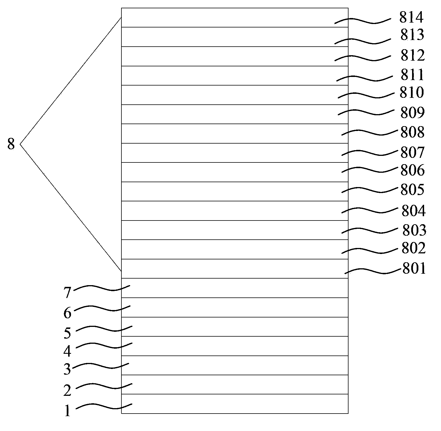
[0060] (1) Pre-treatment of ITO glass substrate 1: cleaning with acetone→cleaning with ethanol→cleaning with deionized water→cleaning with ethanol, all of which are cleaned with an ultrasonic cleaner for 5 minutes in a single wash, then blown dry with nitrogen, and dried in an oven for later use; The cleaned ITO glass substrate 1 also needs surface activation treatment to increase the oxygen content of the conductive surface layer and improve the work function of the conductive layer surface; the thickness of ITO is 100nm;
[0061] (2) Preparation of functional layer and light-emitting layer: hole injection layer 2: evaporate MoO on ITO glass substrate 1 3 Hybrid material obtained by doping NPB, MoO 3 The doping mass fraction is 30%, and the evaporation is carried out by high-vacuum coating equipment, and the vacuum degree during evaporation is 1×10 -5 Pa, the evaporation ra...
Embodiment 2
[0078] A method for preparing an organic electroluminescent device, comprising the following steps:
[0079] (1), (2), (3) are the same as embodiment 1;
[0080] (4) Preparation of protective layer: CuPc was prepared on the cathode layer by vacuum evaporation method, vacuum degree 1×10 -5 Pa, evaporation rate Thickness 200nm;
[0081] (5) Preparation of barrier layer:
[0082] (a) Preparation of the first organic barrier layer: prepared on a PET film, the first organic barrier layer is polytetrafluoroethylene, prepared by spin coating first and then exposed, prepared in an inert atmosphere, and the coating thickness is 1.5 μm. Then use UV light (λ=365nm) to cure, the light intensity is 15mW / cm 2 , exposure time 300s;
[0083] (b) Preparation of oxide layer: prepared on the first organic barrier layer, the oxide layer material is SiO 2 , prepared by magnetron sputtering, the background vacuum is 1×10 -5 Pa, thickness 150nm;
[0084] (c) Preparation of the second organi...
Embodiment 3
[0091] A method for preparing an organic electroluminescent device, comprising the following steps:
[0092] (1), (2), (3) are the same as embodiment 1;
[0093] (4) Preparation of protective layer: prepare Alq on the cathode layer by vacuum evaporation 3 , vacuum degree 5×10 -5 Pa, evaporation rate Thickness 250nm;
[0094] (5) Preparation of barrier layer:
[0095] (a) Preparation of the first organic barrier layer: prepared on a PET film, the first organic barrier layer is methylcyclopentenolone, prepared by spin coating and then exposed, prepared in an inert atmosphere, the coating thickness is 1μm, then cured with UV light (λ=365nm), light intensity 10mW / cm 2 , exposure time 200s;
[0096] (b) Preparation of oxide layer: prepared on the first organic barrier layer, the oxide layer material is TiO 2 , prepared by magnetron sputtering, the background vacuum is 5×10 -5 Pa, thickness 100nm;
[0097] (c) Preparation of the second organic barrier layer: prepared on th...
PUM
| Property | Measurement | Unit |
|---|---|---|
| thickness | aaaaa | aaaaa |
| thickness | aaaaa | aaaaa |
| thickness | aaaaa | aaaaa |
Abstract
Description
Claims
Application Information
 - R&D
- Intellectual Property
- Life Sciences
- Materials
- Tech Scout
- Unparalleled Data Quality
- Higher Quality Content
- 60% Fewer Hallucinations
Browse by: Latest US Patents, China's latest patents, Technical Efficacy Thesaurus, Application Domain, Technology Topic, Popular Technical Reports.
© 2025 PatSnap. All rights reserved.Legal|Privacy policy|Modern Slavery Act Transparency Statement|Sitemap|About US| Contact US: help@patsnap.com