

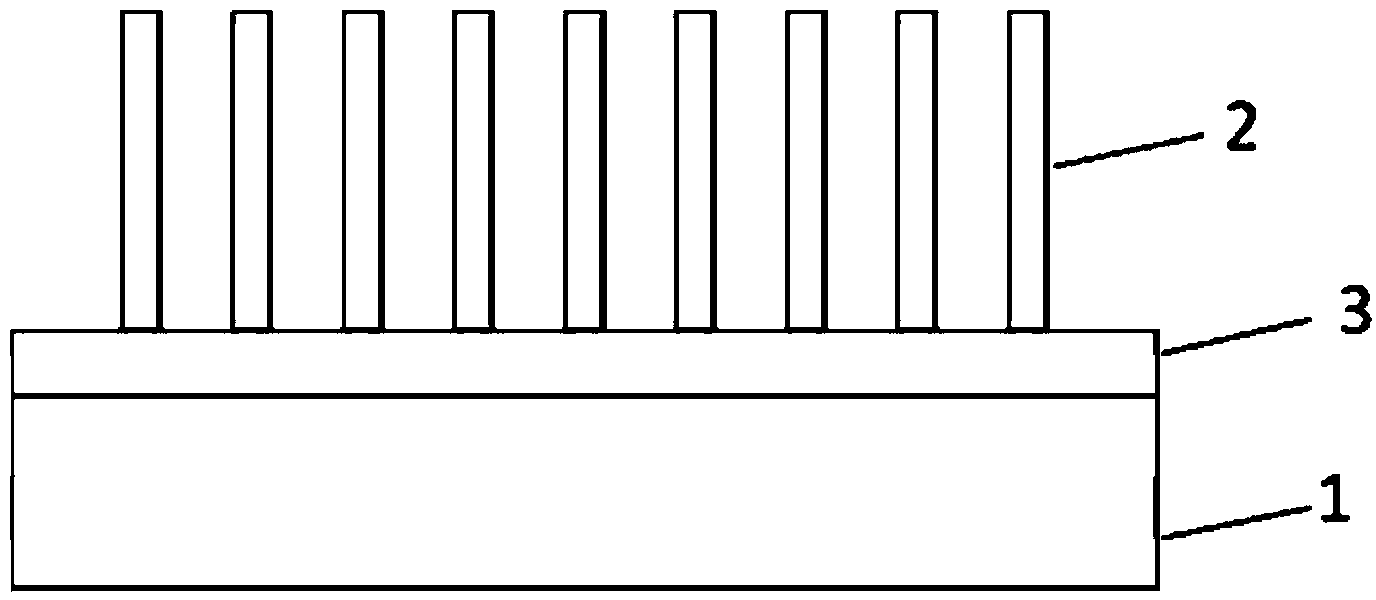
Growth method of GaN nanowire
A growth method and nanowire technology, applied in the growth field of GaN nanowires and GaN nanowires, can solve the problems of high price, difficult to prepare large-size sapphire substrates, and not suitable for large-scale applications, and achieve the purpose of avoiding contamination. Effect
- Summary
- Abstract
- Description
- Claims
- Application Information
AI Technical Summary
Problems solved by technology
Method used
Image

Examples
Embodiment 1
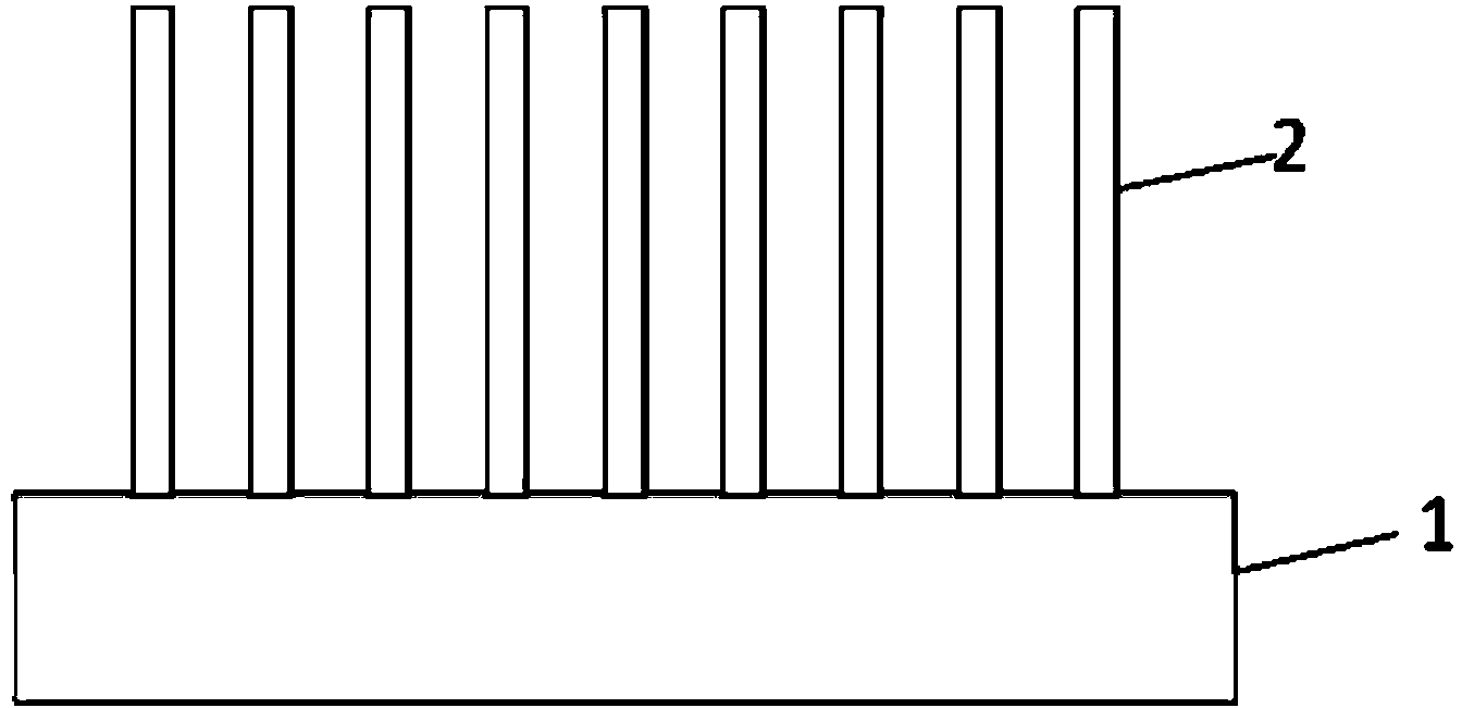
[0037] Sample pattern diagram of GaN nanowires grown on quartz substrate figure 2 As shown, from bottom to top are, quartz substrate, GaN nanowire; its preparation method is:
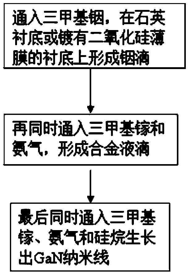
[0038] 1) Put the quartz substrate into the MOCVD reaction chamber, and heat-treat the substrate at 1000°C for 15 minutes in a hydrogen atmosphere;
[0039] 2) At 700°C, with a bias voltage of 400mbar, trimethylindium (TMIn) was injected for 30s, and liquid indium droplets were formed on the substrate with a density of about 8×10 6 piece / cm 2 ;
[0040] 3) Then feed ammonia gas and trimethylgallium (TMGa) at the same time, the molar flow rate of trimethylgallium is 60 μmol / min, the molar flow rate of ammonia gas is 50 times that of trimethylgallium, and GaN is formed and dissolved in indium droplets , forming alloy droplets with a droplet diameter of 100-300nm;
[0041] 4) Finally, ammonia gas, trimethylgallium (TMGa) and silane are introduced at the same time. The flow rate of ammonia gas and trim...
Embodiment 2
[0043] Sample pattern diagram of GaN nanowires grown on quartz substrate figure 2 As shown, from bottom to top are, quartz substrate, GaN nanowire; its preparation method is:
[0044] 1) Put the quartz substrate into the MOCVD reaction chamber, and heat-treat the substrate at 1000°C for 20 minutes in a hydrogen atmosphere;
[0045] 2) At 600°C, with a bias voltage of 350mbar, trimethylindium (TMIn) was pre-introduced for 150s to form liquid-phase indium droplets on the substrate with a density of about 6×10 7 piece / cm 2 ;
[0046] 3) Then feed ammonia gas and trimethylgallium (TMGa) at the same time, the molar flow rate of trimethylgallium is 60 μmol / min, and the molar flow rate of ammonia gas is 100 times that of trimethylgallium, so that GaN is formed and dissolved in indium drops, forming alloy droplets with a diameter of 100-300nm;
[0047] 4) Finally, ammonia gas, trimethylgallium (TMGa) and silane are introduced at the same time. The flow rate of ammonia gas and tri...
Embodiment 3
[0049] Sample pattern diagram of GaN nanowires grown on quartz substrate figure 2 As shown, from bottom to top are quartz substrate and GaN nanowire. Its preparation method is:
[0050] 1) Put the quartz substrate into the MOCVD reaction chamber, and heat-treat the substrate at 1100°C for 20 minutes in a hydrogen atmosphere;
[0051] 2) At 600°C, with a bias voltage of 450mbar, trimethylindium (TMIn) was introduced for 300s to form liquid indium droplets on the substrate with a density of about 5×10 8 piece / cm 2 ;
[0052] 3) Then feed ammonia gas and trimethylgallium (TMGa) at the same time, the molar flow rate of trimethylgallium is 80 μmol / min, and the molar flow rate of ammonia gas is 10 times that of trimethylgallium, so that GaN is formed and dissolved in indium drops, forming alloy droplets with a diameter of 400-500nm;
[0053] 4) Finally, ammonia gas, trimethylgallium (TMGa) and silane are introduced at the same time. The flow rate of ammonia gas and trimethylgall...
PUM
| Property | Measurement | Unit |
|---|---|---|
| length | aaaaa | aaaaa |
| diameter | aaaaa | aaaaa |
| height | aaaaa | aaaaa |
Abstract
Description
Claims
Application Information