Method employing ink-jet printing to make crystalline silica solar cell

An inkjet printing, solar cell technology, applied in the direction of replication/marking methods, printing, circuits, etc., can solve the problems of limited printing accuracy, high conductivity, depression, etc., to achieve good uniformity and repeatability, high printing resolution , The effect of printing high resolution

Inactive Publication Date: 2014-05-21
SHANGHAI SHENZHOU NEW ENERGY DEV
View PDF4 Cites 5 Cited by
  • Summary
  • Abstract
  • Description
  • Claims
  • Application Information

AI Technical Summary

Problems solved by technology

The current mass-production screen printing method can print grid lines with a line width of 80-100 μm and a thickness of 15-20 μm. However, due to the limitations of the following situations in screen printing technology, its continuous optimization has reached a technical bottleneck.
First, the aspect ratio of screen printing grid lines is limited, making it difficult to achieve thinner and taller grid lines
Second, screen printing needs to be in direct contact with the silicon wafer, and the fragmentation rate is high, which will affect the application of low-cost thin wafer technology (<160μm or less)
Third, the life of the screen printing screen is about 10,000 times, and each scraper will cause the screen to relax and sag, which obviously limits the printing accuracy
Fourth, during the screen printing process, it is necessary to press the screen scraper to squeeze the metal paste, so it is impossible to ensure that the paste passing through the screen is uniform, resulting in different amounts of paste in different areas of the silicon wafer , thereby affecting the conversion efficiency of the battery
Fifth, screen printing is difficult to achieve low-cost layered metallization while achieving the requirements of low contact resistance and high conductivity
Although this technology has made great progress, there are still a series of problems, such as loss of layer caused by laser ablation, incomplete chemical etching of SiN film, complex electroless plating process, etc.

Method used


Image

  • Method employing ink-jet printing to make crystalline silica solar cell

Examples


Embodiment 1

[0036] A method for making crystalline silicon solar cells by inkjet printing, comprising the following steps:

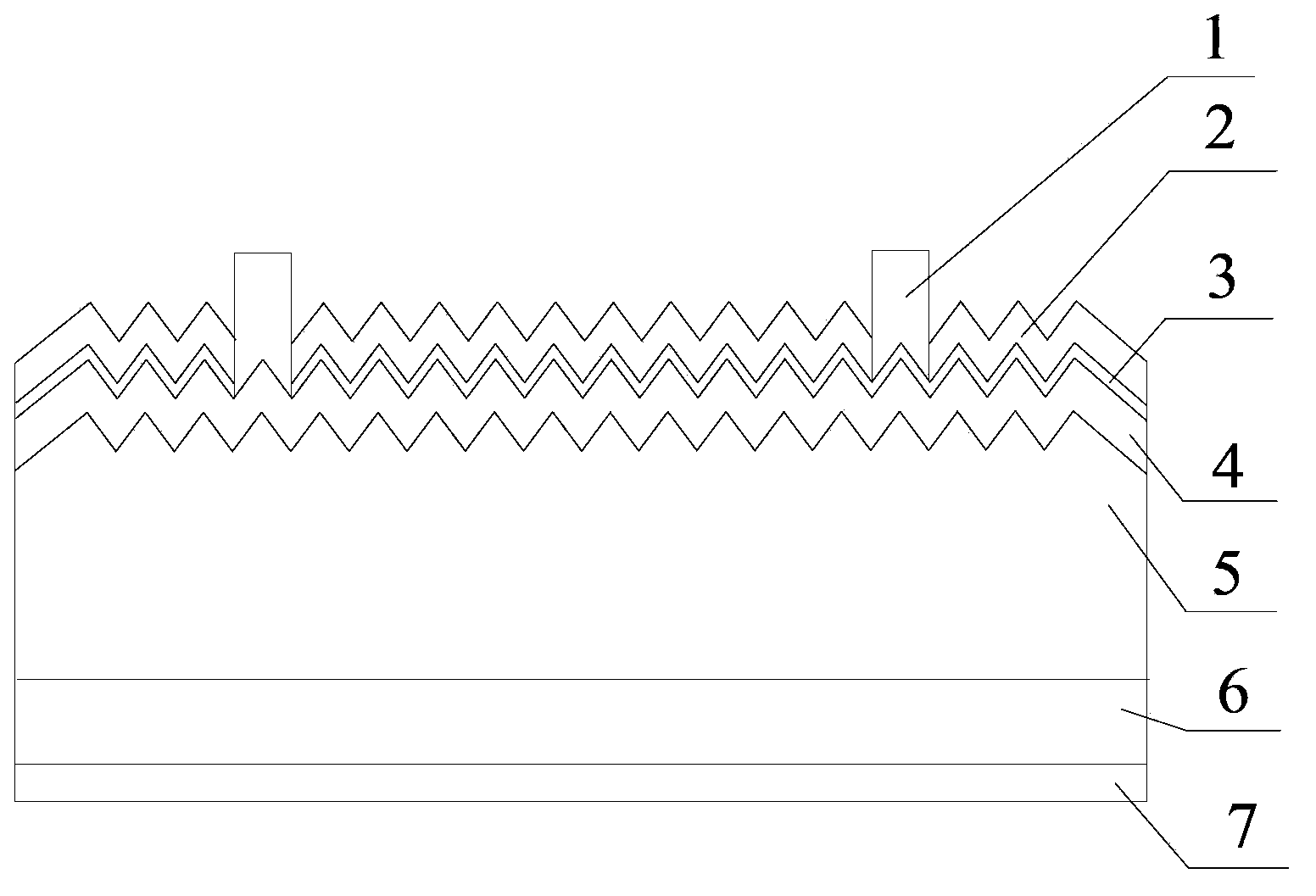
[0037] (1) Cleaning the surface of the P-type monocrystalline silicon wafer and making the textured surface is a surface formed by a pyramid, an inverted pyramid or a pit-like structure with a size of 0.1 to 100 microns;

[0038] (2) performing phosphorus doping on one side of the P-type monocrystalline silicon wafer after texturing to form a PN junction;

[0039] (3) Continue to deposit a layer of passivation and anti-reflection film on the N-type surface;

[0040] (4) Use inkjet printing to achieve surface metallization. Inkjet printing uses the piezoelectric effect of piezoelectric ceramics to make small ink droplets spray onto the surface of the silicon wafer through the nozzle. The diameter of the ink droplet is 30nm. The specific steps are as follows: first Spray printing 20 layers of sub grid line seed layer, and then spray print 50 layers of sub grid line c...

Embodiment 2

[0049] A method for making crystalline silicon solar cells by inkjet printing, comprising the following steps:

[0050] (1) Cleaning the surface of the P-type monocrystalline silicon wafer and making the textured surface is a surface formed by a pyramid, an inverted pyramid or a pit-like structure with a size of 0.1 to 100 microns;

[0051] (2) performing phosphorus doping on one side of the P-type monocrystalline silicon wafer after texturing to form a PN junction;

[0052] (3) Continue to deposit a layer of passivation and anti-reflection film on the N-type surface;

[0053] (4) Inkjet printing is used to achieve surface metallization, and the piezoelectric effect of piezoelectric ceramics is used to spray silver ink onto the surface of the silicon wafer through the nozzle. The diameter of the ink droplet is 20nm. 10 layers of wire seed layer, and then 40 layers of conductive layer for sub-grid lines; then 1 layer of seed layer for busbar lines, and finally 1 layer of condu...

Embodiment 3

[0056] A method for making crystalline silicon solar cells by inkjet printing, comprising the following steps:

[0057] (1) Cleaning the surface of the P-type monocrystalline silicon wafer and making the textured surface is a surface formed by a pyramid, an inverted pyramid or a pit-like structure with a size of 0.1 to 100 microns;

[0058] (2) performing phosphorus doping on one side of the P-type monocrystalline silicon wafer after texturing to form a PN junction;

[0059] (3) Continue to deposit a layer of passivation and anti-reflection film on the N-type surface;

[0060] (4) Inkjet printing is used to achieve surface metallization, and the piezoelectric effect of piezoelectric ceramics is used to spray silver ink onto the surface of the silicon wafer through the nozzle. The diameter of the ink droplet is 40nm. 50 layers of wire seed layer, and then 60 layers of conductive layer for sub-grid lines; then 10 layers of seed layer for busbar lines, and finally 10 layers of c...


PUM

PropertyMeasurementUnit
sizeaaaaaaaaaa
diameteraaaaaaaaaa
widthaaaaaaaaaa

Abstract

The invention relates to a method employing ink-jet printing to make a crystalline silica solar cell; the method comprises the steps of cleaning velvet on a surface of a P type monocrystalline wafer; carrying out phosphor element doping on one surface of the velvet P type monocrystalline wafer so as to form a PN junction; continuously depositing a passivation and anti-reflection film on a N type surface; employing the ink-jet printing to realize surface metallization; carrying out sintering processing making to obtain the crystalline silica solar cell. Compared with the prior art, the method employing ink-jet printing to make the crystalline silica solar cell is high in printing resolution and grid line aspect ratio, uses non-contact printing, realizes layered metallization, is flexible in technology, and good in uniformity and repeatability.

Description

technical field [0001] The invention relates to a method for manufacturing a crystalline silicon solar cell, in particular to a method for manufacturing a crystalline silicon solar cell by inkjet printing. Background technique [0002] A solar cell is a device that converts light energy into electrical energy. At present, solar cells made of crystalline silicon materials account for more than 90% of the market share. Crystalline silicon cells are mainly divided into monocrystalline silicon cells and polycrystalline silicon cells. Since the purity and crystal quality of monocrystalline silicon are higher than those of polycrystalline silicon, the photoelectric conversion efficiency of monocrystalline silicon cells is generally higher than that of polycrystalline silicon solar cells. At present, the technical route of conventional commercial crystalline silicon solar cells is as follows: first, sort the incoming materials, then clean the damaged layer on the surface of crystal...

Claims


Application Information

Patent Timeline
Patent Type & Authority Applications(China)
IPC IPC(8): H01L31/18B41M5/00
CPCB41M5/0047B41M5/0058H01L31/022425H01L31/1804Y02E10/547Y02P70/50
Inventor 胡剑豪张忠卫周利荣马贤芳尹振忠
Owner SHANGHAI SHENZHOU NEW ENERGY DEV
Why Eureka
Try Eureka