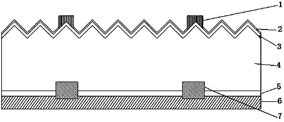
Method for manufacturing back passivation point contact solar cell of aluminum slurry burning-through local thin film
A technology of solar cells and back passivation, which is applied in the direction of circuits, photovoltaic power generation, electrical components, etc., can solve problems such as undetermined process methods, and achieve the effect of reducing equipment investment, saving investment, and simple steps
- Summary
- Abstract
- Description
- Claims
- Application Information
AI Technical Summary
Problems solved by technology
Method used
Image
Examples
Embodiment 1
[0035] A method for preparing a back passivation point contact solar cell in which aluminum paste burns through a local film comprises the following steps:
[0036] (1) De-damage the silicon wafer and make texturing and cleaning: choose 156mmP-type single-crystal silicon wafer as the base material, and its resistivity is 0.5ohm·cm. After de-damaging the selected p-type silicon wafer, use Potassium hydroxide solution chemically etches the surface of the P-type silicon wafer at 45°C to prepare a pyramid-shaped suede surface, which is then cleaned with 0.5% hydrofluoric acid to remove surface impurities;
[0037] (2) Phosphorus diffusion: adopt the method of tubular phosphorus diffusion, specifically in the diffusion furnace at a temperature of 600 ° C, using POCl 3 Phosphorus is diffused on the front side of the silicon wafer to form an n-type layer, so that the square resistance of P-type crystalline silicon is 25ohm / sq, and the naturally formed phosphosilicate glass after diff...
Embodiment 2
[0048] A method for preparing a back passivation point contact solar cell in which aluminum paste burns through a local film comprises the following steps:
[0049](1) De-damage the silicon wafer and make texturing and cleaning: choose 156mm P-type single-crystal silicon wafer as the base material, and its resistivity is 2ohm·cm. After de-damaging the selected p-type silicon wafer, use 5% hydrogen The sodium oxide solution chemically etched the surface of the P-type silicon wafer at 80°C to prepare a pyramid-shaped suede surface, and then cleaned it with 1% hydrofluoric acid to remove surface impurities;
[0050] (2) Phosphorus diffusion: adopt the method of tubular phosphorus diffusion, specifically in the diffusion furnace at a temperature of 800 ° C, using POCl 3 Phosphorus is diffused on the front side of the silicon wafer to form an n-type layer, so that the square resistance of P-type crystalline silicon is 100ohm / sq, and the naturally formed phosphosilicate glass after ...
Embodiment 3
[0061] A method for preparing a back passivation point contact solar cell in which aluminum paste burns through a local film comprises the following steps:
[0062] (1) De-damage the silicon wafer and make texturing and cleaning: choose 156mm P-type single crystal silicon wafer as the base material, and its resistivity is 3ohm·cm, and use hydrogen with a mass fraction of 2.5% after de-damaging the selected p-type silicon wafer Potassium oxide solution chemically etches the surface of the P-type silicon wafer at 65°C to prepare a pyramid-shaped suede surface, which is then cleaned with hydrofluoric acid with a mass fraction of 5% to remove surface impurities;
[0063] (2) Phosphorus diffusion: adopt the method of tubular phosphorus diffusion, specifically in the diffusion furnace at a temperature of 700 ° C, using POCl 3 Phosphorus is diffused on the front side of the silicon wafer to form an n-type layer, so that the square resistance of P-type crystalline silicon is 50ohm / sq,...
PUM
| Property | Measurement | Unit |
|---|---|---|
| thickness | aaaaa | aaaaa |
| thickness | aaaaa | aaaaa |
| thickness | aaaaa | aaaaa |
Abstract
Description
Claims
Application Information
