Hydrogen-passivated zinc oxide-base thin film transistor and preparation method thereof

A thin-film transistor and zinc oxide thin-film technology, which is applied in the direction of transistors, semiconductor/solid-state device manufacturing, semiconductor devices, etc., can solve the problems of poor thermal stability and easy deterioration of device electrical performance, and achieve small hysteresis effect and increase load capacity. Good effect on carrier concentration and electrical stability

Inactive Publication Date: 2014-09-10
WUHAN UNIV
View PDF1 Cites 2 Cited by
  • Summary
  • Abstract
  • Description
  • Claims
  • Application Information

AI Technical Summary

Problems solved by technology

Hydrogen passivation treatment is a common process method to improve the performance of silicon-based thin film transistors, but in the preparation of zinc oxide-based transistors, the electrical properties of the device are easily deteriorated and the thermal stability is deteriorated. avoid hydrogen infiltration

Method used


Image

  • Hydrogen-passivated zinc oxide-base thin film transistor and preparation method thereof
  • Hydrogen-passivated zinc oxide-base thin film transistor and preparation method thereof
  • Hydrogen-passivated zinc oxide-base thin film transistor and preparation method thereof

Examples


Embodiment 1

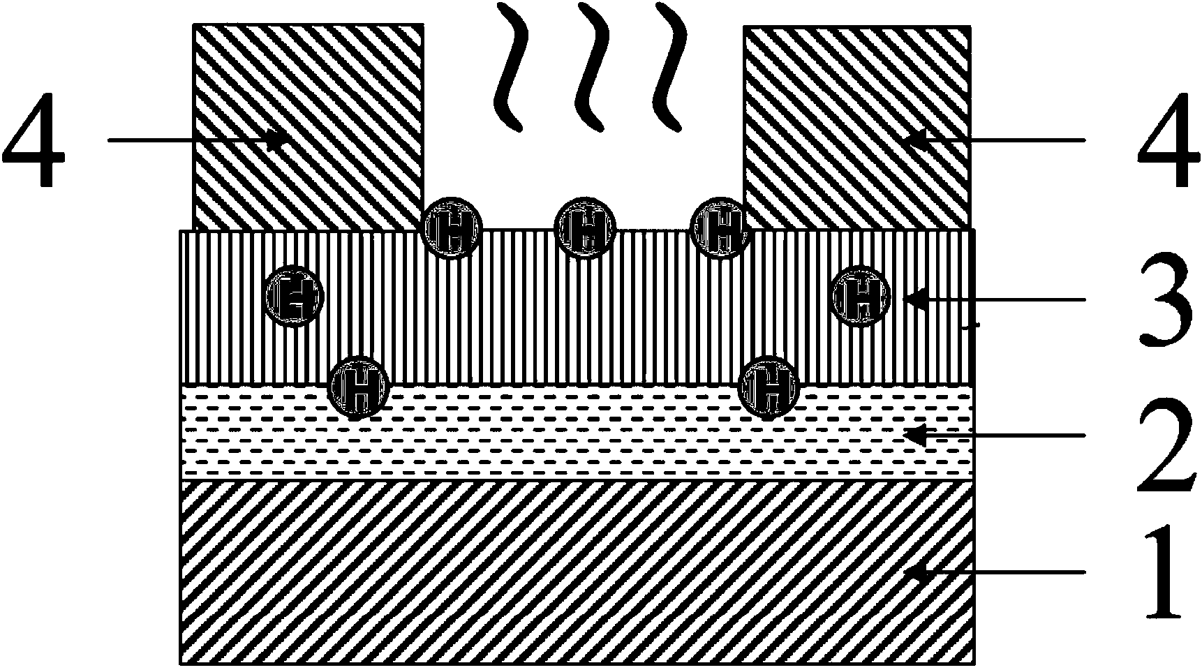
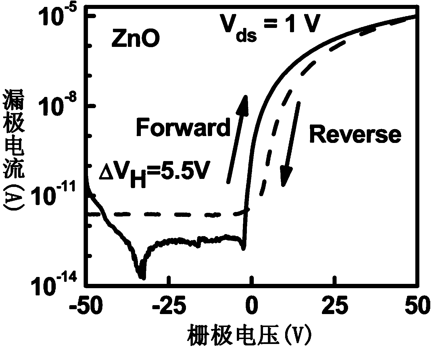
[0039] (1) Silicon wafers grown with 100nm thick silicon dioxide are used as substrates after being ultrasonically cleaned with acetone, isopropanol, deionized water, etc. and blown dry with nitrogen. Under the sputtering carrier gas of argon, a high-purity zinc oxide ceramic target (99.99%) was sputtered with a low-power radio frequency magnetron sputtering of 50 watts, and was divided into small pieces with an area of ​​530 um × 530 um by mask deposition, and To reduce the parasitic capacitance and leakage current introduced in the transistor preparation process, the thickness of the film is controlled to be 15 nanometers by sputtering time. (2) After secondary mask deposition and low-power DC sputtering of 20 watts to form aluminum electrodes, zinc oxide thin film transistors with original electrical properties can be obtained, and their mobility is 10 cm 2 / Vs. image 3 Shown are the transfer characteristic curves of the ZnO TFT in the ranges of -50V to 50V and 50V to -50...

Embodiment 2

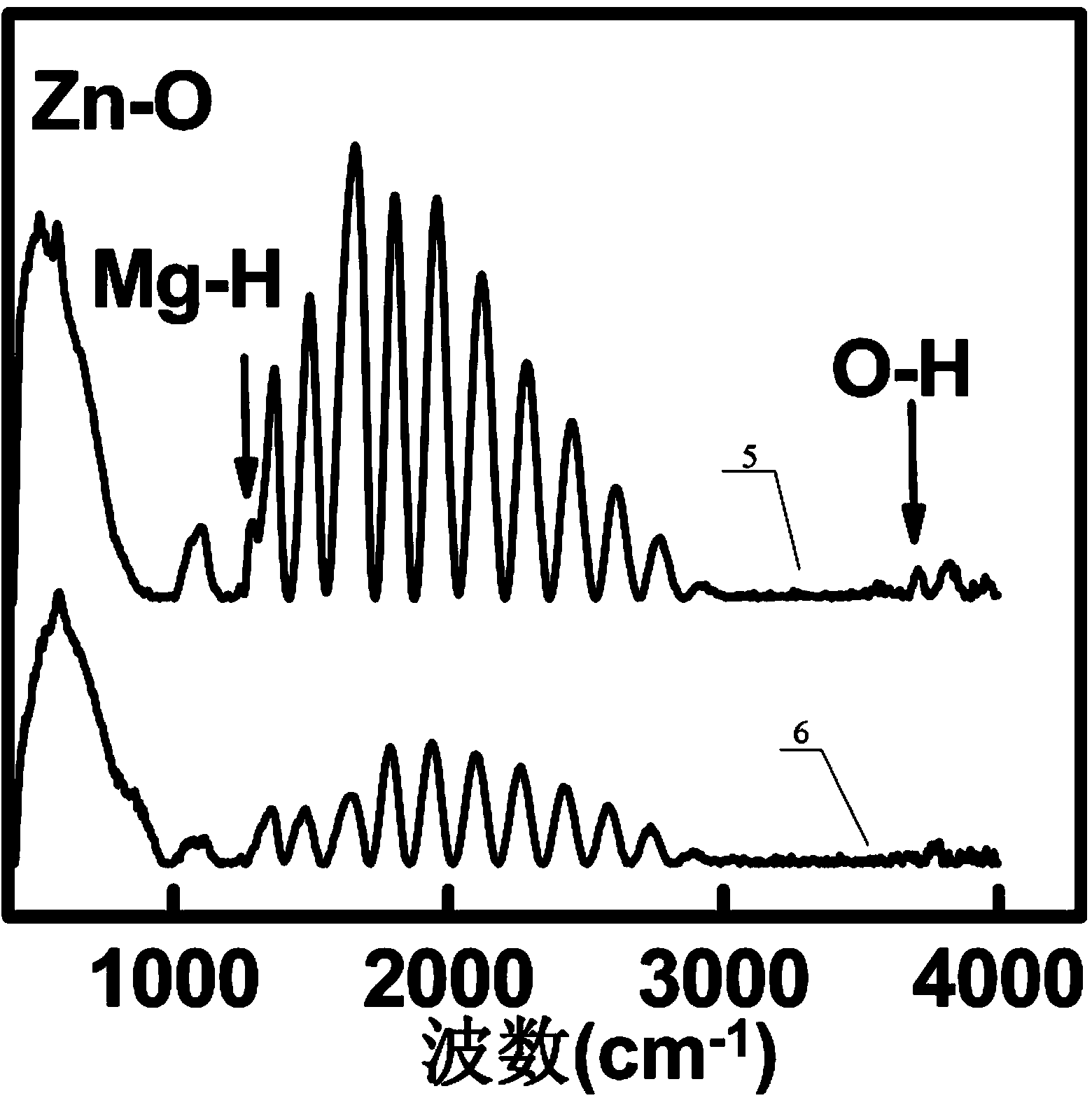
[0041](1) Silicon wafers grown with 100nm thick silicon dioxide are used as substrates after being ultrasonically cleaned with acetone, isopropanol, deionized water, etc. and blown dry with nitrogen. Under the sputtering carrier gas of argon, a high-purity zinc oxide ceramic target (99.99%) was sputtered with a low-power radio frequency magnetron sputtering of 50 watts, and was divided into small pieces with an area of ​​530 um × 530 um by mask deposition, and To reduce the parasitic capacitance and leakage current introduced in the transistor preparation process, the thickness of the film is controlled to be 15 nanometers by sputtering time. (2) After the sputtering is over, close the baffle, and inject a mixed gas of argon and hydrogen (hydrogen accounts for 20% of the total gas) for 30 seconds in situ for hydrogen plasma treatment. (3) After secondary mask deposition and low-power DC sputtering of 20 watts to form aluminum electrodes, a hydrogen-passivated zinc oxide thin f...

Embodiment 3

[0043] (1) Silicon wafers with a thickness of 100 nanometers of silicon dioxide are used as substrates after being ultrasonically cleaned with acetone, isopropanol, deionized water, etc. and blown dry with nitrogen. The temperature of the substrate is 150°C, and the sputtering pressure is 0.6Pa. A high-purity zinc oxide and titanium composite ceramic target (the atomic content of titanium is about 0.5%) was sputtered with a low-power radio frequency magnetron sputtering of 50 watts, and was divided into small pieces with an area of ​​530 um × 530 um by mask deposition to reduce the The parasitic capacitance and leakage current introduced in the preparation process of the small transistor are controlled by the sputtering time to a thickness of 15 nanometers. (2) After the sputtering is over, close the baffle, and inject a mixed gas of argon and hydrogen (hydrogen accounts for 20% of the total gas) for 30 seconds in situ for plasma treatment. (3) A low-power DC sputtering of 20 ...


PUM

PropertyMeasurementUnit
thicknessaaaaaaaaaa
thicknessaaaaaaaaaa

Abstract

The invention discloses a hydrogen-passivated zinc oxide-base thin film transistor. According to the hydrogen-passivated zinc oxide-base thin film transistor, a zinc oxide-base semiconductor material doped with titanium or magnesium and passivated through hydrogen plasma is used as a channel layer. A preparation method of the hydrogen-passivated zinc oxide-base thin film transistor includes the steps that a highly-doped P-type silicon wafer on which silicon dioxide grows is used as a substrate, radio frequency magnetron sputtering is conducted on a composite target of Ti and zinc oxide or Mg and zinc oxide, and meanwhile a small zinc oxide thin film layer doped with Ti or Mg is formed on the substrate through first masking deposition; in-situ hydrogen plasma processing is conducted; direct current sputtering is conducted on the zinc oxide-base thin film layer on which in-situ hydrogen plasma processing is conducted, an Al electrode is prepared through secondary masking deposition, and then the hydrogen-passivated zinc oxide-base thin film transistor is obtained. The hydrogen-passivated zinc oxide-base thin film transistor has the advantages of being high in electron mobility, good in electrical stability, high in switch ratio and the like. The preparation method is simple in process and low in cost, and threshold voltage of a device can be adjusted through hydrogen passivation time and the content of dopants.

Description

technical field [0001] The invention relates to a hydrogen-passivated zinc oxide-based thin film transistor and a preparation method thereof, belonging to the field of nanometer materials and nanometer devices. Background technique [0002] With the advent of the information age, display screens and flexible electronic paper are accelerating towards flat panelization and energy saving. Among them, active array drive display devices with thin film transistors as switching elements have become the best among many flat panel display technologies. A thin film transistor is a field-effect semiconductor device, including several important components such as a substrate, a semiconductor channel layer, an insulating layer, a gate, and source-drain electrodes, among which the semiconductor channel layer is crucial to device performance. [0003] At present, hydrogenated amorphous silicon and polysilicon materials are mainly used for the semiconductor channel layer of commercial thin ...

Claims


Application Information

Patent Timeline
Patent Type & Authority Applications(China)
IPC IPC(8): H01L29/786H01L21/34C23C14/35C23C14/08
CPCH01L29/7869H01L21/0242H01L21/02565H01L21/0257H01L21/02631H01L21/02664H01L29/24H01L29/66969
Inventor 廖蕾许磊刘兴强刘传胜
Owner WUHAN UNIV
Why Eureka
Try Eureka