Friction electric nanometer sensor

A nano-sensor and sensor technology, applied in the field of sensors, achieves the effects of convenient fabrication, cost reduction, and high detection sensitivity

Active Publication Date: 2014-10-01
BEIJING INST OF NANOENERGY & NANOSYST
View PDF3 Cites 39 Cited by
  • Summary
  • Abstract
  • Description
  • Claims
  • Application Information

AI Technical Summary

Problems solved by technology

However, in the field of molecular sensing, there are

Method used


Image

  • Friction electric nanometer sensor
  • Friction electric nanometer sensor
  • Friction electric nanometer sensor

Examples


preparation example Construction

[0103] The present invention also provides a method for preparing the above-mentioned friction nanosensor, comprising the following steps:

[0104] (1) To clean the second conductive element, it can be cleaned with organic solvents and / or water, such as common cleaning agents such as acetone, ether, and ethanol;

[0105] (2) In-situ growth of nanostructures on the surface of the second conductive element to form the second friction layer; wherein the in-situ growth method can be selected according to the different types of the second conductive element and the nanostructure. In order to improve the charge transfer efficiency between the conductive element and the friction layer, it is preferable to use a metal conductive element, and use its corresponding metal oxide as a nanostructure, and the in-situ growth method can use hydrothermal reaction method, epitaxial growth method and electrochemical Etching method, etc.; preferably using hydrothermal reaction method and epitaxial...

Embodiment 1

[0111] Example 1 Catechin (i.e. catechol) sensor

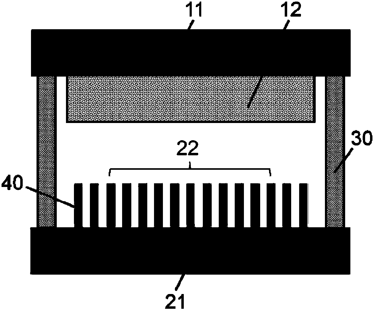
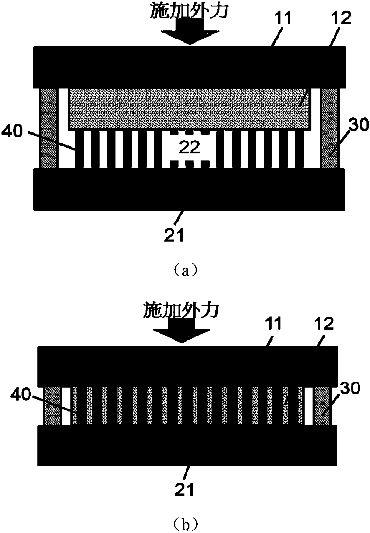
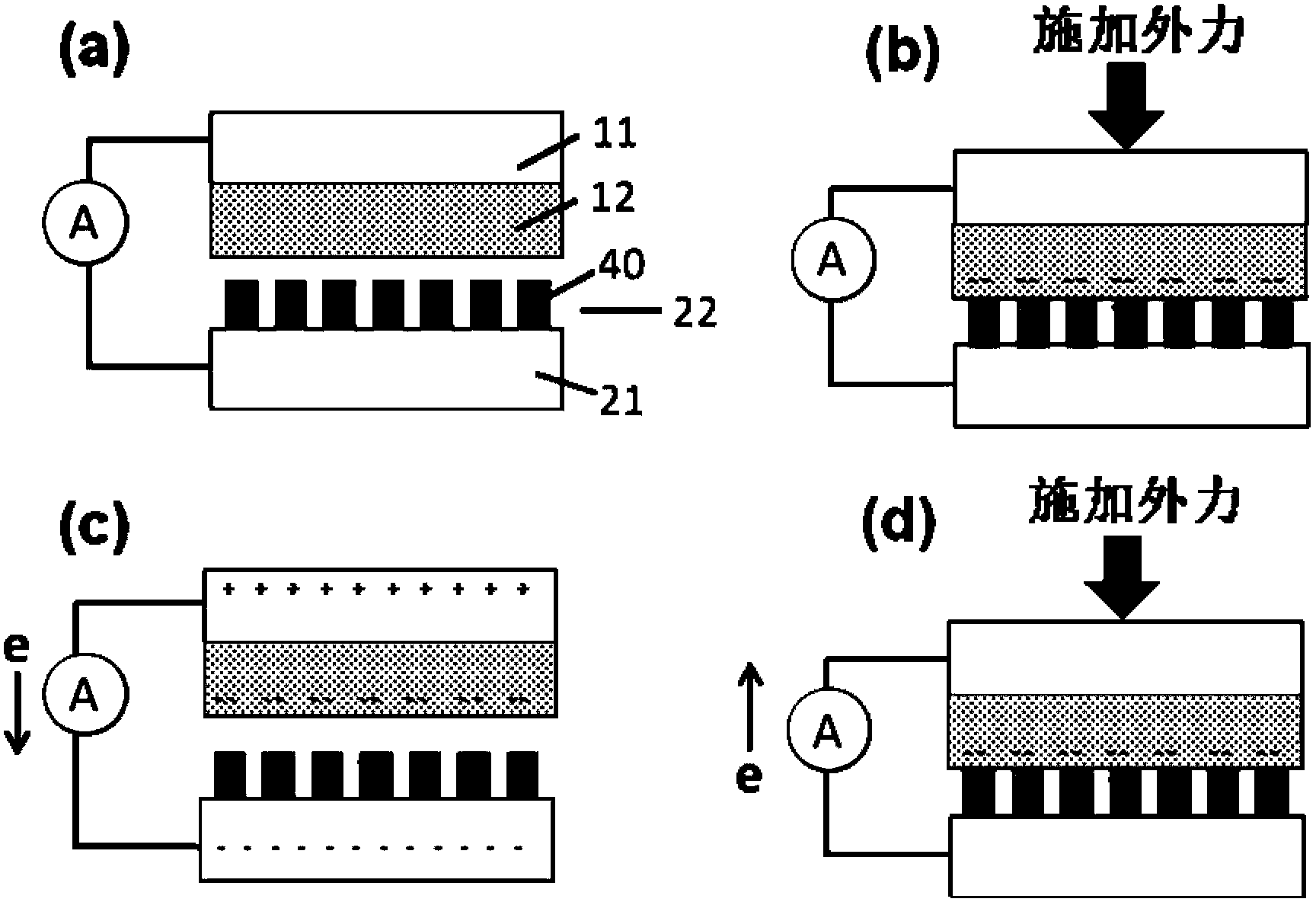
[0112] A metal gold film layer with a thickness of 50nm and a size of 1.8cm×0.6cm is used as the first conductive layer, and a polytetrafluoroethylene (PTFE) film layer with a thickness of 25μm is used as the first friction layer. A metal titanium thin film layer of 1.8cm×0.6cm is used as the second conductive layer, and a titanium dioxide nanowire array with a length of 4.2 μm is grown in situ on the titanium thin film by the hydrothermal method as the second friction layer. This titanium dioxide nanowire array can not only As a friction layer, it can also cause selective adsorption of catechins, and then become a catechin sensor, such as Figure 8 shown. Both the first insulating support layer and the second insulating support layer are plexiglass plates, and the two are connected by springs. For the connection method, see Figure 7 . When no external force is applied on the first support layer or the second support layer...

Embodiment 2

[0114] Embodiment 2 dopamine sensor

[0115] A metal aluminum sheet with a thickness of 5mm and a size of 2cm×2cm is used as the first conductive element, with a thickness of 40μm and a pyramid-shaped polydimethylsiloxane (PDMS) film layer as the first friction layer. A layer of photoresist is spin-coated on the silicon wafer, and a square window array with a side length of micron or sub-micron level is formed on the photoresist by photolithography; the first friction layer after photolithography is completed Chemical etching of hot potassium hydroxide forms a pyramid-shaped array of recessed structures at the window. A metal copper thin plate with a thickness of 5mm and a size of 2cm×2cm was used as the second conductive element, and a ferric oxide nanowire array with a length of 5 μm was grown in situ on it as the second friction layer. Use elastic rubber as an insulating space holder to connect the metal copper sheet and the metal aluminum sheet so that the polydimethylsil...


PUM

PropertyMeasurementUnit
Thicknessaaaaaaaaaa
Sizeaaaaaaaaaa
Thicknessaaaaaaaaaa

Abstract

The invention provides a friction nanometer sensor based on an electron transfer mechanism. The sensor comprises a first conducting element, a second conducting element and a space maintaining element, wherein the lower surface of the first conducting element is in contact with a placed first friction layer; a nanometer structure which directly grows on the upper surface of the second conducting element or is chemically linked with the upper surface of the second conducting element through keys is a second friction layer; the space maintaining element is used for enabling the lower surface of the first friction layer to be realize the face-to-face state with the upper surface of the second friction layer and to maintain a certain distance with the upper surface of the second friction layer; the first friction layer and the second friction layer can be at least in partial contact under the effect of external force, and the original distance is recovered through the effect of the space maintaining element when the external force is withdrawn; meanwhile, electric signals are outwards output through the first conducting element and the second conducting element; and in addition, the electric signals can be changed after the second friction layer is combined with substances of targets to be detected. The sensor has the advantages of self driving performance, high sensitivity, portability and the like.

Description

technical field [0001] The invention relates to a sensor, in particular to a triboelectric nanometer sensor made by utilizing the principle of a friction nanogenerator. Background technique [0002] Today, with the rapid development of microelectronics and material technology, a large number of new microelectronic devices with multiple functions and high integration have been developed continuously, and have shown unprecedented application prospects in various fields of people's daily life. The sensor network will be the fundamental driving force for future economic development. Sensing includes mechanical sensing, chemical sensing, biological sensing and gas sensing. Nanosensor refers to a device that uses sensor devices to convert noteworthy molecular information in the environment (such as heavy metal content or changes in specific biomolecules in the human body) into electrical signals for recording and analysis. With the continuous advancement of science and technolog...

Claims


Application Information

Patent Timeline
IPC IPC(8): G01N27/60B82Y15/00H02N1/04
CPCH02N1/04G01N27/26G01N27/3278B82Y30/00G01N19/02
Inventor 林宗宏王中林
Owner BEIJING INST OF NANOENERGY & NANOSYST
Why Eureka
Try Eureka