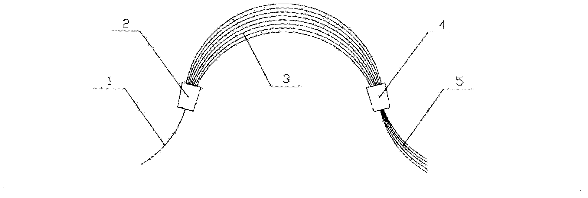
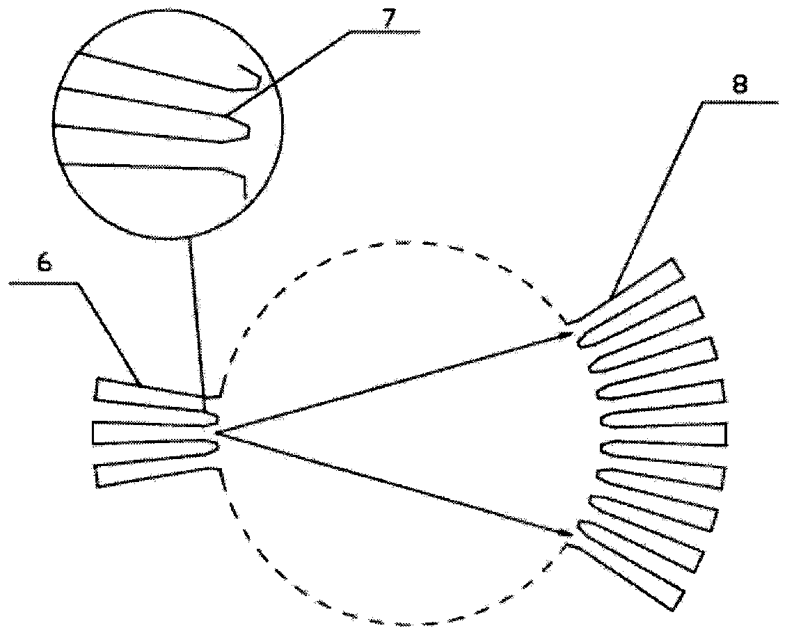
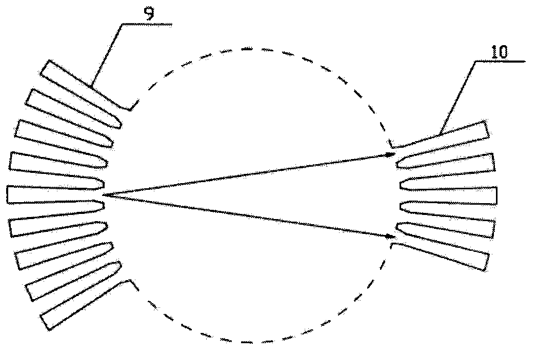
Array raster waveguide type wavelength division multiplexer
A wavelength division multiplexer and array grating technology, applied in the field of integrated optics, can solve the problems of high production cost, difficult design, process, and packaging, and achieve the effects of low cost, light weight and high integration.
- Summary
- Abstract
- Description
- Claims
- Application Information
AI Technical Summary
Problems solved by technology
Method used
Image
Examples
specific Embodiment approach
[0045] The present invention is made by adopting the semiconductor processing technology and process of silicon-based deposited silicon dioxide, such as Figure 3-9 As shown in the schematic diagram of the cross-sectional structure of the planar optical waveguide, it is composed of a silicon-based wafer (11), a liner (12), a waveguide optical core (13) and a cladding layer (16). The process steps are:
[0046] 1. adopt plasma vapor deposition method, on silicon-based wafer (11), deposit liner (12), as Figure 3-2 shown
[0047] 2. adopt plasma vapor deposition method, on liner (12), deposit waveguide optical core (13), as Figure 3-3 shown
[0048] 3. After high-temperature annealing, sputter a layer of chromium (14) on the waveguide optical core (13), such as Figure 3-4 shown
[0049] 4. Coat a layer of photoresist, and complete the photolithography of photoresist by photolithography machine under the mask to form a photoresist image, such as Figure 3-5 shown
[0050]...
PUM
 Abstract
Description
Claims
Application Information


