Nano coarsening composite graphical sapphire substrate and manufacturing method

A sapphire substrate, composite patterning technology, applied in chemical instruments and methods, nanotechnology, crystal growth, etc., can solve the problems of low light extraction efficiency of GaN-based LEDs, increase light extraction efficiency and light output power, and change the propagation. Direction, effects that increase the chance of light escaping

Inactive Publication Date: 2014-12-24
SHANDONG INSPUR HUAGUANG OPTOELECTRONICS
View PDF13 Cites 14 Cited by
  • Summary
  • Abstract
  • Description
  • Claims
  • Application Information

AI Technical Summary

Problems solved by technology

[0010] The present invention aims at the problem of low light extraction efficiency of GaN-based LEDs (light-emitting diodes) that exist in existing patterned sapphire substrates, and provides a n

Method used


Image

  • Nano coarsening composite graphical sapphire substrate and manufacturing method
  • Nano coarsening composite graphical sapphire substrate and manufacturing method
  • Nano coarsening composite graphical sapphire substrate and manufacturing method

Examples


Embodiment 1

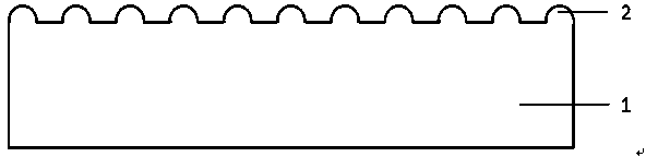
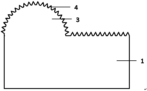
[0036] (1) A micron-scale pattern 2 is prepared on a sapphire substrate 1 .

[0037] Using existing conventional ICP or wet etching method (deposit a layer of silicon dioxide mask on the sapphire substrate; coat a layer of photoresist on the mask layer, use ICP equipment to etch the mask layer to form a mask film pattern; wet etching of sapphire with a mixed solution of sulfuric acid and phosphoric acid.). Micron-scale figures can be hemispheres, pyramids or truncated pyramids, the height of the figure is 1 μm, and the diameter of the bottom surface is 2 μm (the diameter of the bottom surface of the pyramid and prism, that is, its longest diagonal).

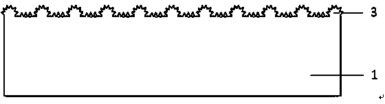
[0038] (2) The substrate is cleaned, and then a silicon dioxide film with a thickness of 200 nm is deposited on the micron-scale pattern 1 .

[0039] (3) Clean the substrate, then deposit a silver film with a thickness of 50nm on the silicon dioxide film, anneal in the air, at a temperature of 300 degrees, and for 1000 seconds, ...

Embodiment 2

[0045] (1) Same as step (1) of Example 1.

[0046] (2) The substrate is cleaned, and then a silicon dioxide film with a thickness of 1000 nm is deposited on the micron-scale pattern 1 .

[0047] (3) on the silicon dioxide film of step (2), deposit the silver thin film of one deck thickness 500nm again; Anneal in oxygen, temperature 900 degree, time 30s, make silver thin film agglomerate and be nano particle, the formed silver nano particle The pattern is an irregular silver nanoparticle pattern with a height of 30nm and a bottom width of 200nm.

[0048] (4) transfer the nanoparticle pattern to the silicon dioxide film by a wet etching pattern transfer method, specifically the aqueous solution of hydrofluoric acid (the volume ratio of hydrofluoric acid and water is 1:5) to transfer the nanoparticle pattern to on the silicon dioxide film.

[0049] (5) Silver nanoparticles are removed by corrosion. The corrosion solution is a mixed solution of ammonia, hydrogen peroxide and wat...

Embodiment 3

[0053] (1) Same as step (1) of Example 1.

[0054] (2) depositing a silicon dioxide film with a thickness of 500nm on the micron-scale pattern formed in step (1);

[0055] (3) On the silicon dioxide film of step (2), deposit a silver film with a thickness of 300nm; anneal in the air, at a temperature of 700 degrees, for 200s, to make the silver film agglomerate and be nanoparticles, which are formed by silver nanoparticles The figure is an irregular silver nanoparticle figure with a height of 155nm and a bottom width of 20nm.

[0056] (4) is the same as the process of step (4) in embodiment (1).

[0057] (5) Silver nanoparticles are removed by corrosion. The corrosion solution is a mixed solution of ammonia, hydrogen peroxide and water. The volume ratio of ammonia and hydrogen peroxide is 3:1, and the volume ratio of the mixture of ammonia and hydrogen peroxide to water is 1:0.2.

[0058] (6) is the same as the process of step (6) in embodiment (1).

[0059] (7) Put the sub...


PUM

PropertyMeasurementUnit
Bottom diameteraaaaaaaaaa

Abstract

Provided are a nano coarsening composite graphical sapphire substrate and a manufacturing method thereof. The sapphire substrate is provided with a composite graphic formed by combining micron dimension graphics with nano dimension graphics, and the nano dimension graphics are arranged on the micron dimension graphics. The manufacturing method includes the steps that (1) the micron dimension graphics are manufactured on the sapphire substrate; (2) a silicon dioxide film is deposited on the micron dimension graphics; (3) a silver film is further deposited on the silicon dioxide film; (4) the silver film is agglomerated into silver nanoparticles; (5) silver nanoparticle graphics are transferred onto the silicon dioxide film; (6) the silver nanoparticles are corroded; (7) the nano dimension graphics are manufactured on the sapphire micron graphics; (8) a silicon dioxide mask layer is removed in a corroded mode; (9) the substrate is cleaned. Nano coarsening is carried out on the micron dimension graphics, the light propagation direction can be changed more efficiently, the light escape probability is increased, and the light extraction efficiency and light output power of a GaN-based LED of the sapphire substrate are improved.

Description

technical field [0001] The invention relates to a nano-roughened composite patterned sapphire substrate for epitaxial growth of GaN crystals and a preparation method thereof, belonging to the technical field of semiconductor crystal preparation. Background technique [0002] GaN has the characteristics of wide direct bandgap, high electron saturation velocity, high breakdown electric field and high thermal conductivity, and has great application potential in the fields of optoelectronics and microelectronics. GaN and other Group III nitrides (InN, AlN) can form a ternary or quaternary solid solution, its forbidden band width is from 0.7eV to 6.28eV, and its emission wavelength is adjustable from infrared to ultraviolet. Get widely used. [0003] Due to the lack of large-scale GaN substrates, GaN thin films are generally grown by heteroepitaxy on substrates such as sapphire, silicon carbide, and silicon. Sapphire is currently the most commonly used substrate for commercial ...

Claims


Application Information

Patent Timeline
IPC IPC(8): H01L33/00H01L33/22C30B33/08B82Y40/00
CPCH01L33/22B82Y40/00C30B33/10H01L33/007
Inventor 王成新徐明升逯瑶曲爽徐现刚
Owner SHANDONG INSPUR HUAGUANG OPTOELECTRONICS
Why Eureka
Try Eureka