Production method of PVDF (polyvinylidene fluoride) ferroelectric field effect transistor based on molybdenum disulfide film

A technology of electric field effect and molybdenum disulfide, which is applied in the direction of circuits, electrical components, electric solid devices, etc., can solve the problems of high switching ratio and unrealizable

Inactive Publication Date: 2015-02-18
SHANGHAI INST OF TECHNICAL PHYSICS - CHINESE ACAD OF SCI
View PDF2 Cites 29 Cited by
  • Summary
  • Abstract
  • Description
  • Claims
  • Application Information

AI Technical Summary

Problems solved by technology

Among many two-dimensional materials, graphene has been extensively studied first, but as a switch

Method used


Image

  • Production method of PVDF (polyvinylidene fluoride) ferroelectric field effect transistor based on molybdenum disulfide film
  • Production method of PVDF (polyvinylidene fluoride) ferroelectric field effect transistor based on molybdenum disulfide film
  • Production method of PVDF (polyvinylidene fluoride) ferroelectric field effect transistor based on molybdenum disulfide film

Examples


Embodiment 1

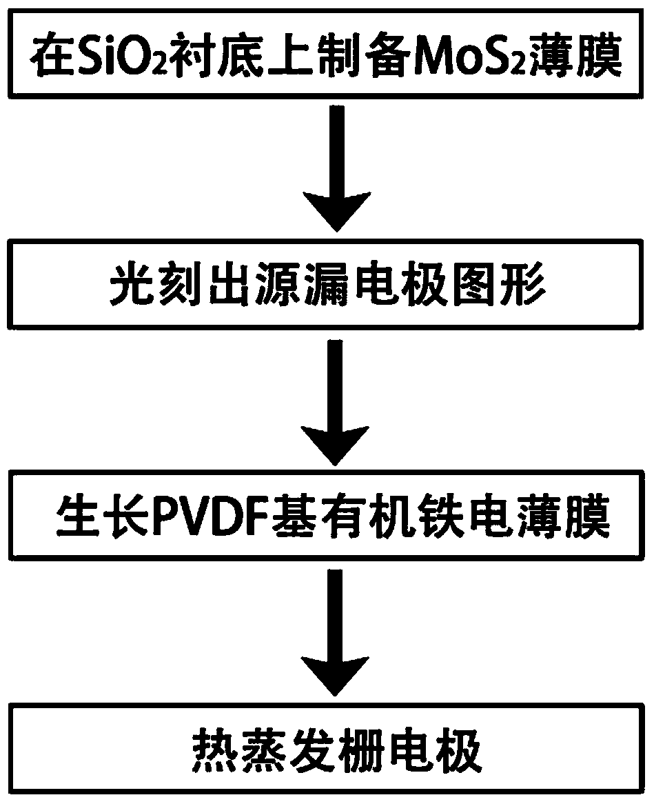
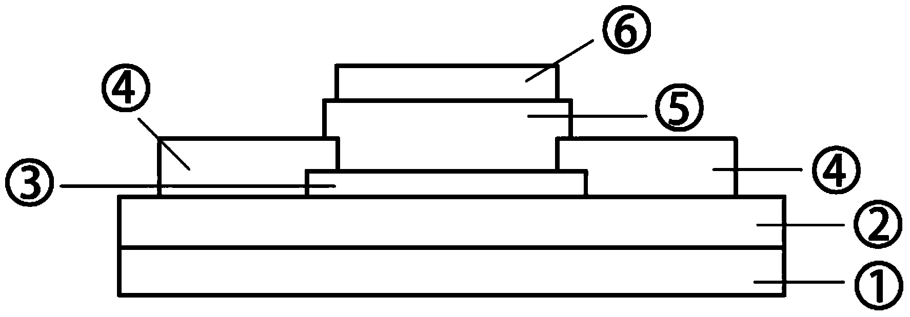
[0024] SiO 2 The substrate material is cleaned to ensure the cleanliness of its surface, and MoS is grown by chemical vapor deposition 2 film. Then in MoS 2 The surface of the film is spin-coated with photoresist, baked, exposed to ultraviolet light, developed, and baked to obtain the required source-drain electrode pattern structure; then the source-drain Au electrode is obtained through thermal evaporation of Au and lift-off steps;

[0025] The rotational speed of the spin-coated photoresist described therein is 4k rpm, the baking temperature is 85 degrees Celsius, and the ultraviolet light exposure time is 20 seconds.

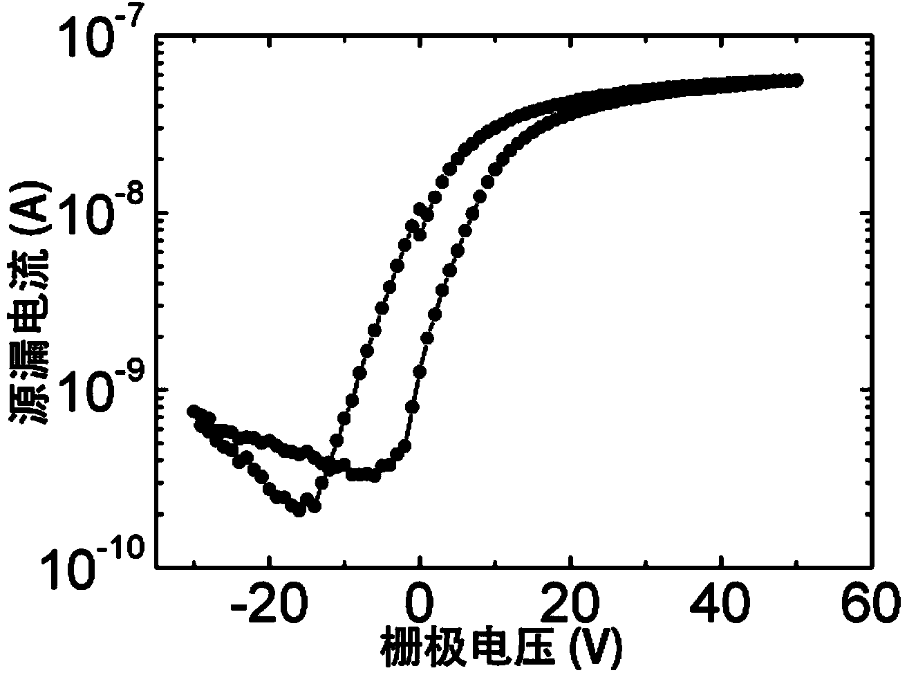
[0026] The PVDF-based polymer P(VDF-TrFE) is dissolved in a dimethyl sulfoxide solution, and the concentration of the solution is 0.01% by mass. Then the P(VDF-TrFE) organic ferroelectric polymer dimethyl sulfoxide solution is evenly spread into the liquid tank of the Langmuir-Brockett device that has been injected into the static ultrapure water, and the...

Embodiment 2

[0032] SiO 2 The substrate material is cleaned to ensure the cleanliness of its surface, and MoS is grown by mechanical exfoliation 2 film. Then in MoS 2 The surface of the film is spin-coated with photoresist, baked, exposed to ultraviolet light, developed, and baked to obtain the required source-drain electrode pattern structure; then the source-drain Au electrode is obtained through thermal evaporation of Au and lift-off steps;

[0033]The rotational speed of the spin-coated photoresist described therein is 4k rpm, the baking temperature is 85 degrees Celsius, and the ultraviolet light exposure time is 20 seconds.

[0034] The PVDF-based polymer P(VDF-TrFE) is dissolved in a dimethyl sulfoxide solution, and the concentration of the solution is 2.5% by mass. Then the P(VDF-TrFE) organic ferroelectric polymer dimethyl sulfoxide solution was transferred layer by layer to MoS by spin coating. 2 A ferroelectric film with a certain thickness is obtained on a patterned substra...


PUM


Abstract

The invention discloses a production method of a PVDF (polyvinylidene fluoride) ferroelectric field effect transistor based on a molybdenum disulfide film. The production method is characterized by including producing the MoS2 (molybdenum disulfide) film on a Si (silicon) substrate of thermal oxide growth SiO2 (silicon dioxide), etching source and drain electrodes of a field effect transistor structure by photoetching and lift off methods, transfers a PVDF organic ferroelectric polymer film onto the MoS2 film with the source and drain electrodes, removing residual solvent on an interface and guaranteeing good crystallization characteristic of the film after annealing treatment, and finally, producing a metal gate electrode by photoetching and etching methods to produce a MoS2 ferroelectric field effect transistor device. The production method has the advantages that the production method for producing the organic ferroelectric field effect transistor structure is simple in technology and guarantees research on ferroelectric polarization control of electronic transport features, related photoelectric devices and related memory devices of MoS2.

Description

technical field [0001] The present invention relates to regulation of MoS 2 The preparation technology of organic ferroelectric field effect transistors with electron transport characteristics, specifically refers to a method based on polyvinylidene fluoride-based organic ferroelectric polymers as the insulating dielectric layer of transistors to regulate MoS 2 Preparation method for electron transport properties. Background technique [0002] In recent years, two-dimensional layered semiconductor materials have received more and more attention due to their excellent electrical, optical, mechanical and other properties. Among many two-dimensional materials, graphene has been extensively studied first. However, as a switching device, graphene cannot achieve a high switching ratio due to the limitation of zero band gap. In contrast, MoS 2 As a typical representative of transition metal sulfides, its single-layer forbidden band width can reach 1.8eV, and the indirect bandgap...

Claims


Application Information

Patent Timeline
IPC IPC(8): H01L51/40H01L51/30H01L51/10
CPCH10K85/10H10K10/00H10K10/80
Inventor 王旭东王建禄孟祥建韩莉孙硕沈宏林铁孙璟兰褚君浩
Owner SHANGHAI INST OF TECHNICAL PHYSICS - CHINESE ACAD OF SCI
Why Eureka
Try Eureka