Production method of single-crystal silicon carbide nanowire high-sensitivity purple-light photoelectric detector
A single crystal silicon carbide, photodetector technology, applied in circuits, electrical components, semiconductor devices, etc., can solve the problems of slow response and recovery time of photodetectors, achieve short recovery time, increase sensitivity, and reduce contact resistance. Effect
- Summary
- Abstract
- Description
- Claims
- Application Information
AI Technical Summary
Problems solved by technology
Method used
Image

Examples
Embodiment 1
[0043] The preparation method of the single crystal silicon carbide nanowire high-sensitivity violet light photodetector in this embodiment, the steps include:
[0044] (1) SiC single crystal substrate cleaning: cut the purchased 3C-SiC single wafer into about 1cm 2 After the square chip is cleaned by the semiconductor standard cleaning process, a certain thickness (5nm) of metal Ni film is evaporated on its surface.
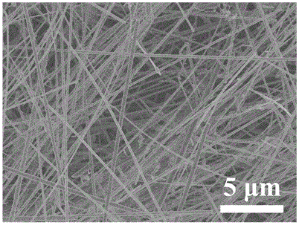
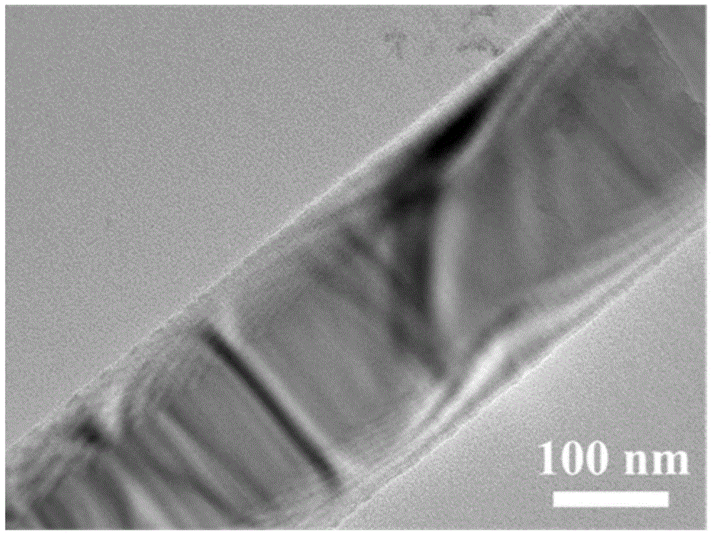
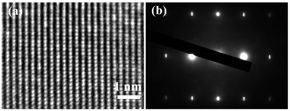
[0045] (2) Preparation of SiC single crystal nanowires: Take 2g of silicon carbon xerogel and grind it in a ball mill for 30min, then put it into a 20mL crucible, place the SiC single wafer directly above the raw material, and seal it with carbon paper . Place the sealed crucible in the center of the vacuum box furnace. Introduce Ar gas and adjust the air flow rate to 200 sccm, set the temperature of the tube furnace to 1400°C, heat up for 1 hour, hold for 1 hour, and then cool down to room temperature naturally with the furnace. figure 1 and 2 Typical scann...
Embodiment 2
[0053] The preparation method of the single crystal silicon carbide nanowire high-sensitivity violet light photodetector in this embodiment, the steps include:
[0054] (1) SiC single crystal substrate cleaning: cut the purchased 3C-SiC single wafer into about 1cm 2 After the square chip is cleaned by the semiconductor standard cleaning process, a certain thickness (30nm) of metal Ni film is evaporated on its surface.
[0055](2) Preparation of SiC single crystal nanowires: Take 2g of silicon carbon xerogel and grind it in a ball mill for 30min, then put it into a 20mL crucible, place the SiC single wafer directly above the raw material, and seal it with carbon paper . Place the sealed crucible in the center of the vacuum box furnace. Introduce Ar gas and adjust the airflow rate to 200 sccm, set the temperature of the tube furnace to 1200°C, the heating time is 1.5 hours, the holding time is 2 hours, and then naturally cool to room temperature with the furnace. figure 1 and...
Embodiment 3
[0059] The preparation method of the single crystal silicon carbide nanowire high-sensitivity violet light photodetector in this embodiment, the steps include:
[0060] (1) SiC single crystal substrate cleaning: cut the purchased 3C-SiC single wafer into about 1cm 2 After the square chip is cleaned by the semiconductor standard cleaning process, a certain thickness (20nm) metal Ni film is evaporated on its surface.
[0061] (2) Preparation of SiC single crystal nanowires: Take 2g of silicon carbon xerogel and grind it in a ball mill for 30min, then put it into a 20mL crucible, place the SiC single wafer directly above the raw material, and seal it with carbon paper . Place the sealed crucible in the center of the vacuum box furnace. Introduce Ar gas and adjust the airflow rate to 200 sccm, set the temperature of the tube furnace to 1000°C, the heating time is 0.5 hours, the holding time is 1 hour, and then naturally cool to room temperature with the furnace. figure 1 and 2...
PUM
| Property | Measurement | Unit |
|---|---|---|
| thickness | aaaaa | aaaaa |
| thickness | aaaaa | aaaaa |
| thickness | aaaaa | aaaaa |
Abstract
Description
Claims
Application Information
 - R&D
- Intellectual Property
- Life Sciences
- Materials
- Tech Scout
- Unparalleled Data Quality
- Higher Quality Content
- 60% Fewer Hallucinations
Browse by: Latest US Patents, China's latest patents, Technical Efficacy Thesaurus, Application Domain, Technology Topic, Popular Technical Reports.
© 2025 PatSnap. All rights reserved.Legal|Privacy policy|Modern Slavery Act Transparency Statement|Sitemap|About US| Contact US: help@patsnap.com