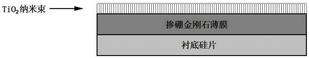
TiO2 nano-beam/boron-doped diamond film composite photoelectrocatalysis electrode and preparation method and application thereof
A technology of boron-doped diamond and photoelectric catalysis, which is applied in the field of preparation of TiO2 nanobeam/boron-doped diamond film composite photocatalytic electrode and composite photocatalytic electrode, which can solve the problem of photocatalytic performance that needs to be improved, high equipment requirements and complicated preparation process and other problems, to achieve the effect of shortening the degradation time, increasing the contact area, and overcoming easy aggregation
- Summary
- Abstract
- Description
- Claims
- Application Information
AI Technical Summary
Problems solved by technology
Method used
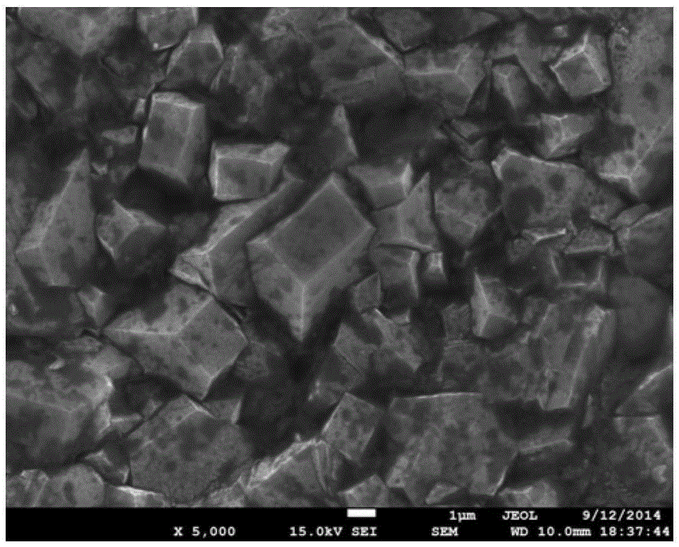
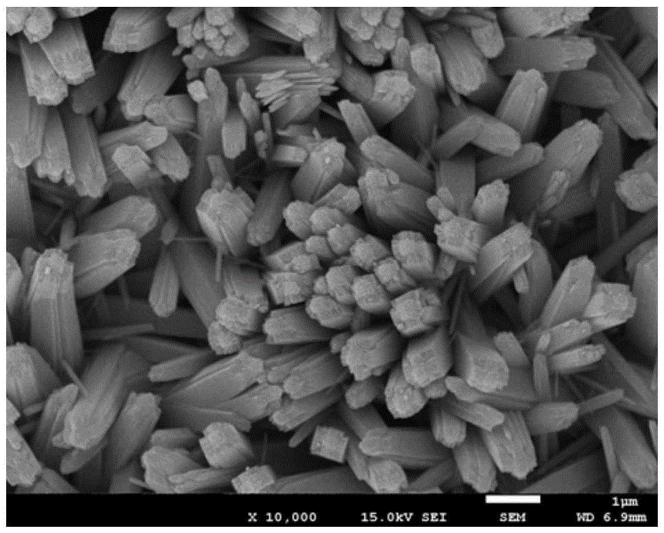
Image

Examples
Embodiment 1
[0028] TiO 2 The nanobeam / boron-doped diamond film composite photoelectrocatalytic electrode, its preparation steps are as follows:
[0029] 1) Take a silicon substrate (silicon wafer, purity 99.999%) and ultrasonically clean it with absolute ethanol, acetone, and ultrapure water for 10 minutes to remove impurities such as oxides on the surface of the substrate; then place the cleaned substrate on The suspension containing diamond powder (mixed powder with a particle size greater than 5nm and less than 250nm) was ultrasonically cleaned for 1 hour to form tiny, dense pits and nucleation defects on the surface of the substrate to reduce the free energy of nucleation; The bottom was ultrasonically cleaned with absolute ethanol and ultrapure water for 10 minutes respectively, and then dried with nitrogen after cleaning;
[0030] 2) Place the above-mentioned silicon substrate (substrate) in a microwave plasma chemical vapor deposition reaction chamber, use diborane as a boron sour...
Embodiment 2
[0035] TiO 2 The nanobeam / boron-doped diamond film composite photoelectrocatalytic electrode, its preparation steps are as follows:
[0036] 1) Take a silicon substrate (silicon wafer, purity 99.999%) and ultrasonically clean it with absolute ethanol, acetone, and ultrapure water for 10 minutes to remove impurities such as oxides on the surface of the substrate; then place the cleaned substrate on The suspension containing diamond powder (mixed powder with a particle size greater than 5nm and less than 250nm) was ultrasonically cleaned for 1 hour to form tiny, dense pits and nucleation defects on the surface of the substrate to reduce the free energy of nucleation; The bottom was ultrasonically cleaned with absolute ethanol and ultrapure water for 10 minutes respectively, and then dried with nitrogen after cleaning;
[0037] 2) Place the above-mentioned silicon substrate (substrate) in a microwave plasma chemical vapor deposition reaction chamber, use diborane as a boron sour...
Embodiment 3
[0040] TiO 2 The nanobeam / boron-doped diamond film composite photoelectrocatalytic electrode, its preparation steps are as follows:
[0041] 1) Take a silicon substrate (silicon wafer, purity 99.999%) and ultrasonically clean it with absolute ethanol, acetone, and ultrapure water for 10 minutes to remove impurities such as oxides on the surface of the substrate; then place the cleaned substrate on The suspension containing diamond powder (mixed powder with a particle size greater than 5nm and less than 250nm) was ultrasonically cleaned for 1 hour to form tiny, dense pits and nucleation defects on the surface of the substrate to reduce the free energy of nucleation; The bottom was ultrasonically cleaned with absolute ethanol and ultrapure water for 10 minutes respectively, and then dried with nitrogen after cleaning;
[0042] 2) Place the above-mentioned silicon substrate (substrate) in a microwave plasma chemical vapor deposition reaction chamber, use diborane as a boron sour...
PUM
| Property | Measurement | Unit |
|---|---|---|
| thickness | aaaaa | aaaaa |
| width | aaaaa | aaaaa |
Abstract
Description
Claims
Application Information
 - R&D
- Intellectual Property
- Life Sciences
- Materials
- Tech Scout
- Unparalleled Data Quality
- Higher Quality Content
- 60% Fewer Hallucinations
Browse by: Latest US Patents, China's latest patents, Technical Efficacy Thesaurus, Application Domain, Technology Topic, Popular Technical Reports.
© 2025 PatSnap. All rights reserved.Legal|Privacy policy|Modern Slavery Act Transparency Statement|Sitemap|About US| Contact US: help@patsnap.com