Self-driven wide-spectral-response silicon-based hybrid heterojunction photoelectric sensor and preparation method therefor

A photoelectric sensor, wide-spectrum technology, applied in photovoltaic power generation, electric solid-state devices, semiconductor/solid-state device manufacturing, etc., can solve the problems of difficult oxide thickness and thin film, high device preparation cost, high dependence, etc., to reduce defects density of states, improved separation and transmission efficiency, and reduced fabrication costs

Active Publication Date: 2016-06-29
JINAN UNIVERSITY
View PDF8 Cites 14 Cited by
  • Summary
  • Abstract
  • Description
  • Claims
  • Application Information

AI Technical Summary

Problems solved by technology

However, thermal evaporation or electron beam evaporation is more difficult to accurately control the thickness of oxides and internal defects of the film, and coating methods such as thermal evaporation are more dependent on equipment, resulting in high device manufacturing costs

Method used


Image

  • Self-driven wide-spectral-response silicon-based hybrid heterojunction photoelectric sensor and preparation method therefor
  • Self-driven wide-spectral-response silicon-based hybrid heterojunction photoelectric sensor and preparation method therefor
  • Self-driven wide-spectral-response silicon-based hybrid heterojunction photoelectric sensor and preparation method therefor

Examples


Embodiment 1

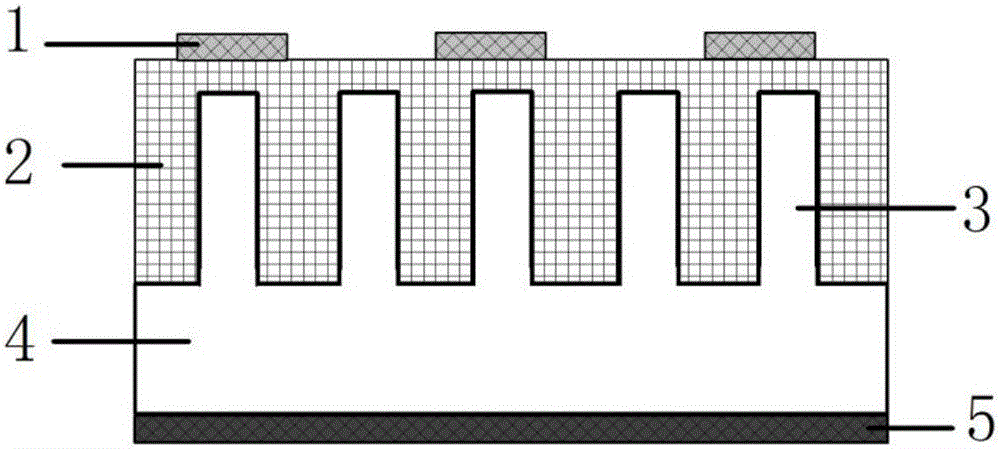
[0050] This embodiment discloses a self-driven wide-spectrum response silicon-based hybrid heterojunction photosensor, which is an alkylated organic / inorganic hybrid heterojunction photosensor, including a metal back electrode 5 , N-type silicon substrate 4, N-type silicon nanowire array 3, organic polymer semiconductor film 2 and sensor anode 1 (front metal gate electrode).

[0051] The upper surface of the N-type silicon substrate 4 is etched into an N-type silicon nanowire array 3, and then a layer of organic polymer semiconductor film 2 is covered on the surface of the N-type silicon nanowire array 3, and the surface of the organic polymer semiconductor film 2 is provided with The positive electrode 1 of the sensor is used as the positive electrode of the battery; the lower surface of the N-type silicon substrate 4 is provided with a thin film as a metal back electrode 5, which can form a good ohmic contact with silicon and play a good role in collecting electrons.

[0052...

Embodiment 2

[0062] This embodiment discloses a method for preparing a self-driven wide-spectrum response silicon-based hybrid heterojunction photoelectric sensor, that is, the method for preparing the above-mentioned organic semiconductor film-silicon heterojunction photoelectric sensor, including the following steps:

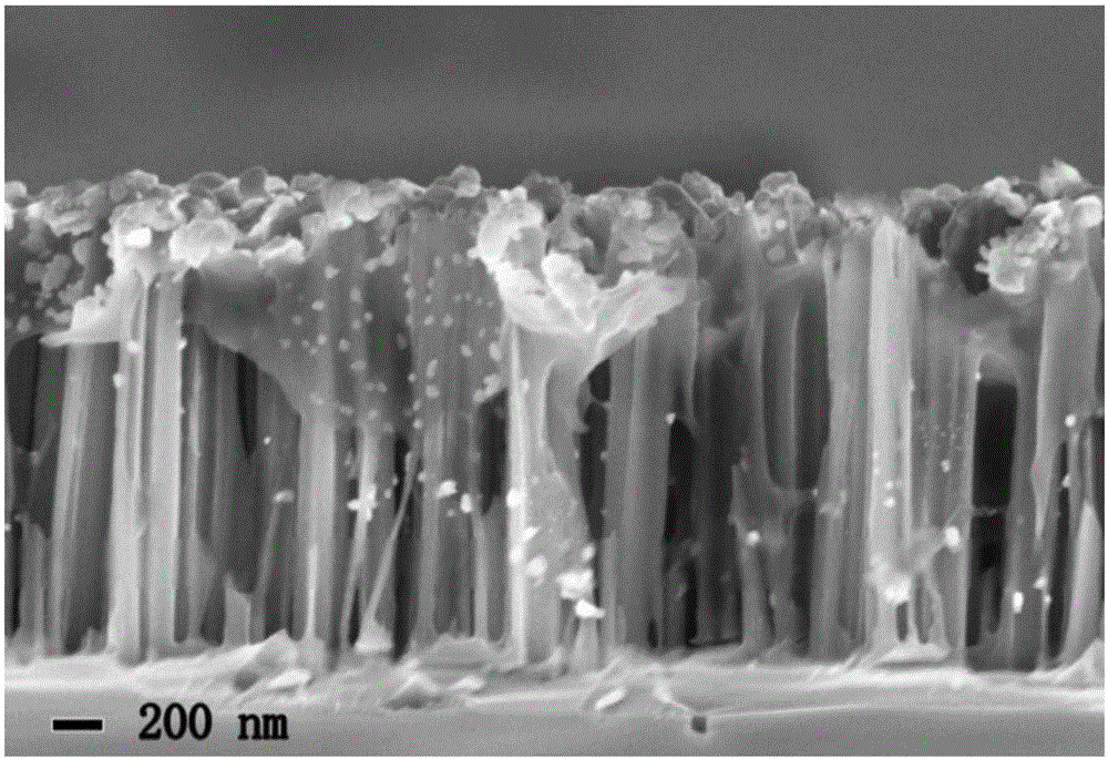
[0063] S1, using the metal-assisted chemical reaction etching method to process the clean N-type single crystal silicon substrate to obtain the N-type silicon substrate 4 of the silicon nanowire array;

[0064] S2, using hydrofluoric acid (HF) to remove the oxide layer on the surface of the N-type silicon substrate 4 treated in step S1;

[0065] S3. Alkylation treatment is performed on the surface of the N-type silicon substrate 4 treated in step S2 to obtain a passivated surface of the N-type silicon nanowire array 3 structure.

[0066] S4. Uniformly spin coating an organic solution on the alkylated N-type silicon nanowire array 3 . In an inert atmosphere, under the cond...

Embodiment 3

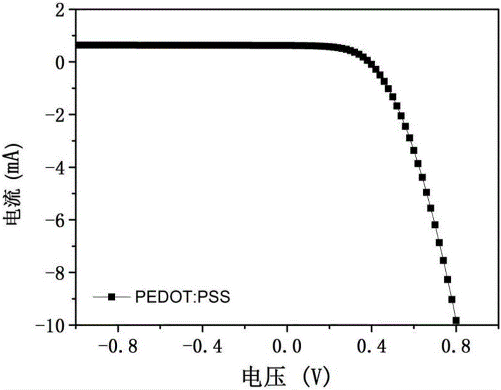
[0073] This embodiment discloses a method for preparing a self-driven wide-spectrum response silicon-based hybrid heterojunction photoelectric sensor, that is, a method for preparing the above-mentioned organic semiconductor thin film PEDOT:PSS-silicon heterojunction photosensor:

[0074] SA1. Use commercialized double-sided polishing, N-type single crystal silicon wafer with a resistivity of 1-10 ohms per centimeter and a crystal orientation of 100; clean the silicon wafer with RCA standard cleaning method, and then dry it with nitrogen to obtain N-type silicon substrate;

[0075] Put the cleaned planar silicon substrate into 4.8M HF and 0.02M AgNO 3 In the mixed solution, silicon nanowire arrays with different lengths are obtained by controlling the reaction and different etching times at normal temperature. The length of the nanowires is about 10 min in the optimized process, the length of the nanowires is about 1 μm, and the distance between the nanowires is 50 nm to 450 ...


PUM

PropertyMeasurementUnit
lengthaaaaaaaaaa
thicknessaaaaaaaaaa
thicknessaaaaaaaaaa

Abstract

The invention discloses a self-driven wide-spectral-response silicon-based hybrid heterojunction photoelectric sensor and a preparation method therefor. The photoelectric sensor comprises a metal back electrode, an N type silicon substrate, an N type silicon nanowire array, an organic polymer semiconductor thin film and a sensor positive electrode, wherein the hybrid photoelectric sensor is characterized in that the N type silicon nanowire array and the organic polymer semiconductor thin film form three-dimensional heterojunction contact, so that the transmission path of photo-generated carriers is effectively shortened; the separation efficiency is improved; a surface / interface composite effect is reduced through interface alkylation processing; the silicon-based micro-nano structure is taken as the main light absorption layer and the generation and transmission layers for the photo-generated carriers as well; and a P type organic semiconductor thin film is processed to be used as a hole transport layer. The photoelectric sensor provided by the invention has the characteristics of self powering, wide spectral response, low cost large-area preparation, high photoelectric response speed and the like.

Description

technical field [0001] The invention relates to the technical field of photoelectric sensing, in particular to a self-driven wide-spectrum response silicon-based hybrid heterojunction photoelectric sensor and a preparation method thereof. Background technique [0002] Photoelectric sensors are widely used in military and civilian products such as optical communication, optical fiber sensing, laser ranging, tracking guidance, automatic control, forest fire prevention, environmental monitoring, and scientific research. [0003] Photoelectric sensors can be divided into photoconductive sensors, photovoltaic sensors and photon emission sensors. Generally speaking, thin-film photoconductive sensors are easy to manufacture and low in cost, but their disadvantages are slow response, difficult array control, and high power consumption. Photon emission sensors have fast response speed, but their disadvantages are high production cost, large equipment dependence and high power consum...

Claims


Application Information

Patent Timeline
Patent Type & Authority Applications(China)
IPC IPC(8): H01L51/42H01L51/48B82Y40/00
CPCB82Y40/00H10K71/231H10K71/30H10K30/00Y02E10/549Y02P70/50
Inventor 赵传熙谢伟广麦文杰刘彭义梁智敏
Owner JINAN UNIVERSITY
Why Eureka
Try Eureka