Preparation method for surface-enhanced Raman substrate and surface-enhanced Raman substrate structure

A surface-enhanced Raman and substrate structure technology, applied in Raman scattering, measuring devices, instruments, etc., can solve the problems of small substrate area, large area of ​​contaminated substrate, difficulty in ensuring consistency, and high preparation cost. Achieve high sensitivity, simple and convenient preparation method, and low cost

Inactive Publication Date: 2016-08-10
INST OF PHYSICS - CHINESE ACAD OF SCI
View PDF8 Cites 14 Cited by
  • Summary
  • Abstract
  • Description
  • Claims
  • Application Information

AI Technical Summary

Problems solved by technology

However, this method has many disadvantages, including the pollution of metal particles by chemical reagents in the synthesis process and the difficulty in ensuring the large area and consistency of the substrate.
In addition, metal nanostructure substrates can also be prepared by electron beam exposure technology. The substrate area produced by this preparation method is relatively small and the preparation cost is relatively high.

Method used


Image

  • Preparation method for surface-enhanced Raman substrate and surface-enhanced Raman substrate structure
  • Preparation method for surface-enhanced Raman substrate and surface-enhanced Raman substrate structure
  • Preparation method for surface-enhanced Raman substrate and surface-enhanced Raman substrate structure

Examples


preparation example Construction

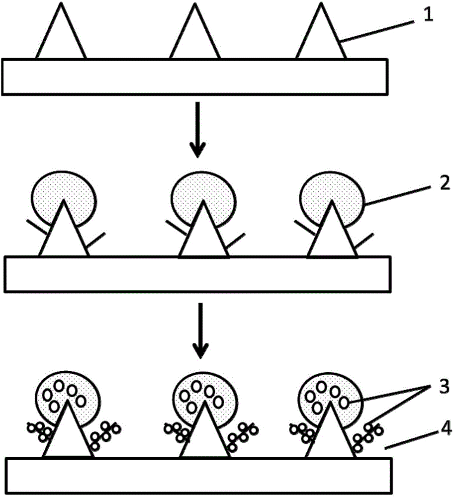
[0032] figure 1 It is a process flow diagram of a method for preparing a surface-enhanced Raman substrate 4 according to an embodiment of the present invention. see figure 1 , the present invention provides a method for preparing a surface-enhanced Raman substrate 4, forming a composite structure with surface-enhanced Raman characteristics through graphene nanosheets 2 and metal particles 3, comprising the following steps:

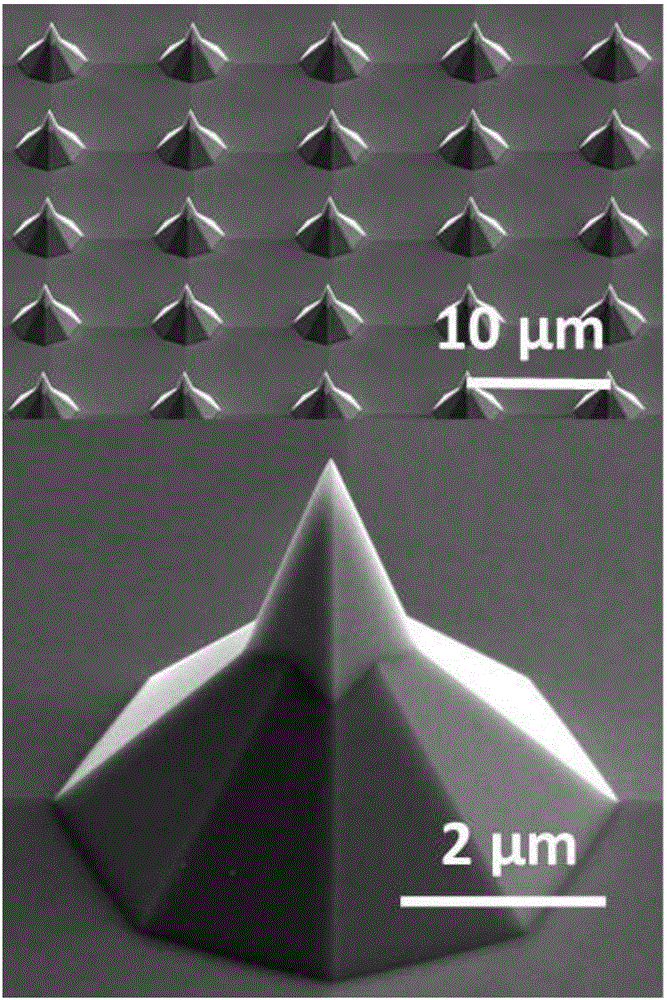
[0033] Step 1. Select a silicon substrate and etch the silicon substrate to prepare a silicon pyramid array 1 . Such as Figure 2a SEM side view of the sample after step 1 is shown.

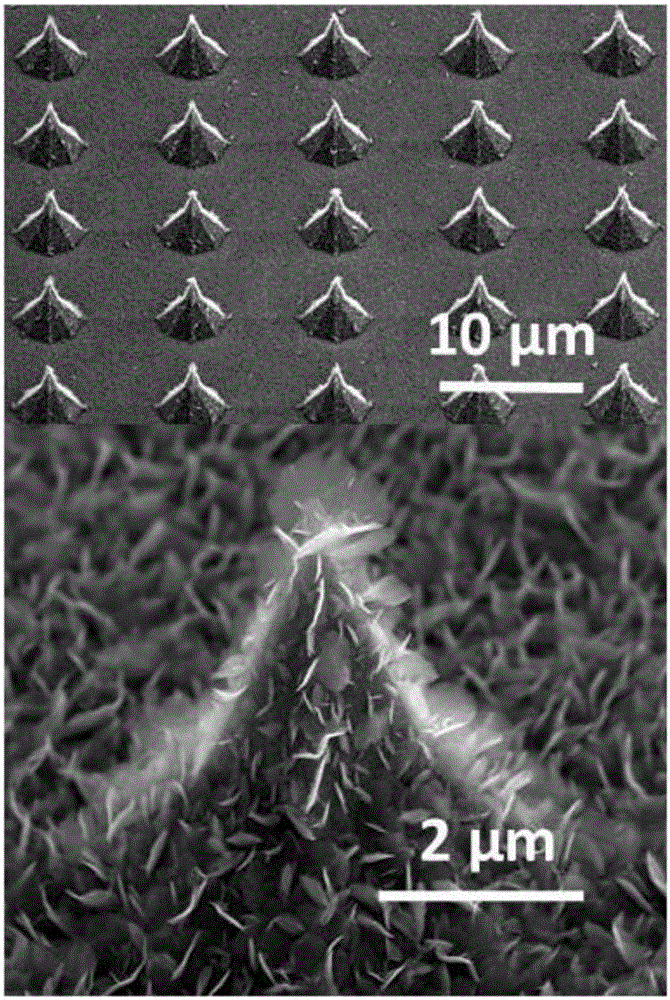
[0034] Step 2, putting the silicon pyramid array 1 into a microwave plasma chemical vapor deposition system to grow graphene nanosheets 2 . Such as Figure 2b SEM side view of the sample after step 2 is shown.

[0035] Step 3, coating a layer of metal particles 3 on the surface of the graphene nanosheet 2, so that the surface-enhanced Raman substrate 4 can be obtained. ...

Embodiment 1

[0049] see figure 1, select a silicon (100) substrate, where 100 is the crystal plane of silicon, deposit a 60nm thick silicon nitride film on the silicon (100) substrate, and perform photolithography, etching, and wet etching on the silicon nitride film To prepare the silicon pyramid array 1; put the silicon pyramid array 1 into the microwave plasma chemical vapor deposition (MPCVD) system, the basic vacuum is 0.1Pa, the gas flow ratio of methane and hydrogen is 2:1, and the air pressure is 600Pa keep it for 3min, and grow graphene nanosheets 2; use DC magnetron sputtering to deposit a Ag film with a thickness of 3nm on the graphene nanosheets 2, the basic vacuum is 5E-9Torr, the speed of the sample stage is 10rpm, and the sputtering power It is 100W, and the working air pressure is 0.004Torr.

[0050] Figure 3a It is a scanning electron microscope side view of the front of one of the graphene nanosheets 2 of the surface-enhanced Raman substrate 4 prepared in Example 1 of ...

Embodiment 2

[0052] see figure 1 , select a silicon (100) substrate, where 100 is the crystal plane of silicon, deposit a 60nm thick silicon nitride film on the silicon (100) substrate, and perform photolithography, etching, and wet etching on the silicon nitride film To prepare the silicon pyramid array 1; put the silicon pyramid array 1 into a microwave plasma chemical vapor deposition (MPCVD) system, the basic vacuum is 0.1Pa, the gas flow ratio of methane and hydrogen is 3:1, and the air pressure is 600Pa keep it for 3min, grow graphene nanosheets 2; use DC magnetron sputtering to deposit a Ag film with a thickness of 5nm on the graphene nanosheets 2, the basic vacuum is 5E-9Torr, the sample stage speed is 10rpm, and the sputtering power It is 100W, and the working air pressure is 0.004Torr.

[0053] Figure 4a It is a scanning electron microscope side view of the front of one of the graphene nanosheets 2 of the surface-enhanced Raman substrate 4 prepared in Example 2 of the present ...


PUM

PropertyMeasurementUnit
diameteraaaaaaaaaa
diameteraaaaaaaaaa

Abstract

The invention provides a method for preparing a surface-enhanced Raman substrate and a surface-enhanced Raman substrate structure, and relates to the field of preparation of micro-nano structures. The preparation method includes: selecting a silicon substrate and etching the silicon substrate to prepare a silicon pyramid array; putting the silicon pyramid array into a microwave plasma chemical vapor deposition system to grow graphene nanosheets; The surface of the sheet is coated with a layer of metal particles, so that a surface-enhanced Raman substrate can be obtained. The surface-enhanced Raman substrate structure is prepared by the preparation method. The preparation method of the present invention can prepare a large-area and uniform surface-enhanced Raman substrate, and ensures the purity of metal particles to avoid contamination. Simultaneously, the preparation method of the present invention is simple and convenient, and the cost is also low. The surface-enhanced Raman substrate prepared by the invention has strong Raman enhancement characteristics and extremely high sensitivity.

Description

technical field [0001] The invention relates to the field of preparation of micro-nano structures, in particular to a preparation method of a surface-enhanced Raman substrate and a surface-enhanced Raman substrate structure. Background technique [0002] Surface-enhanced Raman Scattering (SERS) is widely used in molecular detection and analysis in the fields of chemistry, biology, and medicine because it can realize non-destructive testing, fingerprint identification, and has high sensitivity. In recent years, the needle-tip Raman-enhanced scattering technology developed on the basis of surface Raman-enhanced scattering has also achieved high-sensitivity exploration at the single-molecule level. With the development of micro-nano processing technology, the chip of surface Raman enhanced scattering substrate has also been commercialized, so it is expected to be more widely used in many research and detection fields. [0003] In surface-enhanced Raman scattering, the substrat...

Claims


Application Information

Patent Timeline
Patent Type & Authority Applications(China)
IPC IPC(8): G01N21/65
CPCG01N21/658
Inventor 李俊杰王玉瑾全保刚顾长志
Owner INST OF PHYSICS - CHINESE ACAD OF SCI
Why Eureka
Try Eureka