IGBT device manufacturing method and device

A manufacturing method and device technology, applied in semiconductor/solid-state device manufacturing, semiconductor devices, electrical components, etc., can solve the problems of high MOSFET channel resistance, increased cost, and insufficient reliability of gate oxide, and achieve the goal of overcoming impurity doping, cost saving effect

Pending Publication Date: 2016-09-28
JILIN SINO MICROELECTRONICS CO LTD
View PDF9 Cites 2 Cited by
  • Summary
  • Abstract
  • Description
  • Claims
  • Application Information

AI Technical Summary

Problems solved by technology

[0004] There are two main technical problems in the design of wide bandgap semiconductor IGBT devices: one is the low channel electron mobility, which leads to the problem of large channel resistance of MOSFET; the other is the insufficient reliability of gate oxide under high temperature and high electric field. Therefore, the main technical problem in the design of wide bandgap semiconductor IGBT devices lies in the above-mentioned technical problems faced by wide bandgap semiconductor MOSFET devices
[0006] One is to choose a suitable crystal orientation, because the electron mobility of different crystal orientations is different, and the mobility can differ by up to 5 times, so the crystal surface with high electron mobility is selected to form a channel; because the crystal orientation of silicon carbide is chaotic, so Crystal faces with high electron mobility are not easy to choose
[0007] The second is to improve the state of the channel interface

Method used


Image

  • IGBT device manufacturing method and device
  • IGBT device manufacturing method and device
  • IGBT device manufacturing method and device

Examples


Embodiment Construction

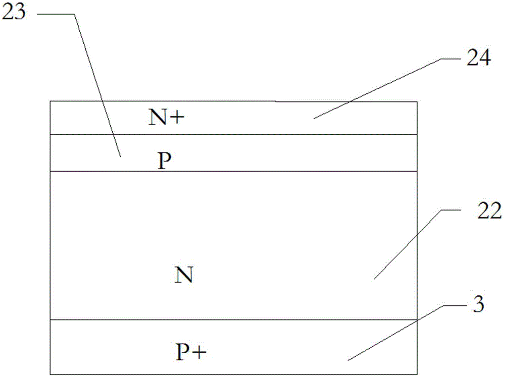
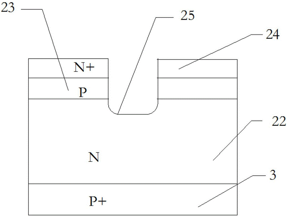
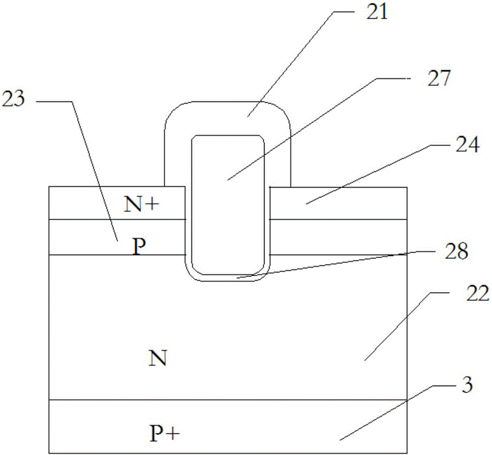
[0062] The technical solutions of the present invention will be clearly and completely described below in conjunction with the accompanying drawings. Apparently, the described embodiments are some of the embodiments of the present invention, but not all of them. Based on the embodiments of the present invention, all other embodiments obtained by persons of ordinary skill in the art without making creative efforts belong to the protection scope of the present invention.

[0063] In the description of the present invention, it should be noted that the orientation or positional relationship indicated by the terms "center", "upper", "lower", "left", "right", "inner" and "outer" are based on the attached The orientation or positional relationship shown in the figure is only for the convenience of describing the present invention and simplifying the description, and does not indicate or imply that the referred device or element must have a specific orientation, be constructed and ope...


PUM

PropertyMeasurementUnit
Thicknessaaaaaaaaaa

Abstract

The invention relates to the technical field of a semiconductor device, and especially relates to an IGBT device manufacturing method and device. The method comprises the following steps: carrying out epitaxy on a P+ substrate through epitaxy technology to obtain a voltage withstand drift region, a P-type body area epitaxial layer and an N+ source region epitaxial layer in sequence, which form a base body; through photoetching and etching technique, providing a gate trench and a Schottky groove in the base body; carrying out thermal oxidation on the inner wall of the gate trench to form a gate oxide layer; forming a gate electrode on the inner wall of the gate oxide layer through deposition, photoetching and etching; carrying out passivation layer deposition on the outer surface of the gate electrode, and forming a gate electrode insulation protection layer through photoetching and etching; lastly, carrying out Schottky barrier metal deposition and annealing on the surface of the Schottky groove to form a Schottky diode; and finally, obtaining an IGBT device. According to the IGBT device manufacturing method and device, impurity doping and diffusion processes are saved, and reliability of the gate oxide layer is enhanced.

Description

technical field [0001] The invention relates to the technical field of semiconductor devices, in particular to a method for manufacturing an IGBT device and the device. Background technique [0002] Wide bandgap semiconductor IGBT devices, especially silicon carbide IGBT devices and gallium nitride IGBT devices, are power switching devices that have attracted much attention at present. Its driving circuit is very simple and has good compatibility with existing power device driving circuits. . [0003] IGBT (Insulated Gate Bipolar Transistor) is a composite fully-controlled voltage-driven power semiconductor device composed of BJT (Bipolar Transistor) and MOSFET (Metal Oxide Semiconductor Transistor), which combines the high input impedance of MOSFET and BJT (also known as GTR) has the advantages of low conduction voltage drop. Among them, the vertical IGBT device and the P-type emission area on the back of the chip are mainly realized by ion implantation technology and epi...

Claims


Application Information

Patent Timeline
IPC IPC(8): H01L21/331H01L29/739H01L29/06
CPCH01L29/0607H01L29/66325H01L29/66348H01L29/7393H01L29/7397
Inventor 刘广海叶武阳宋宏德邢文超贾国
Owner JILIN SINO MICROELECTRONICS CO LTD
Why Eureka
Try Eureka