Bi-metal sulfur group ternary semiconductor nanoparticle and preparation method thereof

A nanoparticle and semiconductor technology, applied in the field of biomedicine, can solve the problems of few reports of bimetallic chalcogenide ternary semiconductor nanomaterials, poor water solubility and biocompatibility, and complicated preparation process, and achieves easy promotion and uniform particle size. , the effect of simple operation

Active Publication Date: 2017-01-04
SUZHOU UNIV
View PDF2 Cites 12 Cited by
  • Summary
  • Abstract
  • Description
  • Claims
  • Application Information

AI Technical Summary

Problems solved by technology

The preparation process of these methods is relatively complicated, the conditions are relatively harsh, and the resulting products are large in size, poor in water solubility and biocompatibility, so that the application of bimetallic chalcogenide ternary semiconductor nanomaterials in biomedicine is rarely reported.

Method used


Image

  • Bi-metal sulfur group ternary semiconductor nanoparticle and preparation method thereof
  • Bi-metal sulfur group ternary semiconductor nanoparticle and preparation method thereof
  • Bi-metal sulfur group ternary semiconductor nanoparticle and preparation method thereof

Examples


Embodiment 1

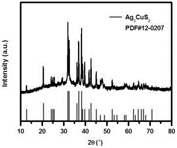
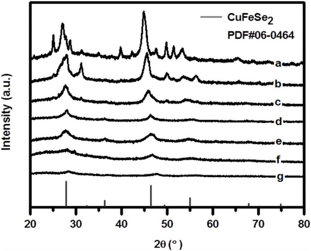
[0049] After passing 100mL of ultrapure water through nitrogen to remove oxygen, weigh sodium borohydride (2.27g, 60mmol) and add it to the anaerobic water to dissolve completely, then add selenium powder (1.57g, 20mmol), the molar ratio of sodium borohydride to selenium 3:1, after the selenium powder reacts completely, dissolve 5mL of CuCl 2 2H 2 O and FeSO 4 ·7H 2 O (the total molar weight of the two is 20mmol, the addition ratio is nFe / n(Cu+Fe)=0.2(b), 0.4(c), 0.5(d), 0.6(e), 0.8(f), single CuCl 2 2H 2 O, single FeSO 4 ·7H 2 O (g)) aqueous solution is injected into the selenium precursor, and the solution turns black immediately, is centrifuged and washed, and vacuum-dried to obtain a black powder. The X-ray diffraction (XRD) of the obtained copper-iron-selenium semiconductor nanoparticles is shown in figure 1 . from figure 1 It can be seen that the resulting CuFeSe 2 (d) Diffraction peaks of nanoparticles and CuFeSe 2 -XRD standard cards are consistent, and the d...

Embodiment 2

[0051] After passing 100mL of ultrapure water through nitrogen to remove oxygen, weigh sodium borohydride (2.27g, 60mmol) and add it to the anaerobic water to dissolve completely, then add selenium simple substance (1.57g, 20mmol), the molar ratio of sodium borohydride to selenium simple substance 3:1, after the selenium powder reacts completely, dissolve 5mL of CuCl 2 2H 2 O (1.70mg, 10mmol) and NiCl 2 ·6H 2 The aqueous solution of O (2.38g, 10mmol) was injected into the selenium precursor solution, and the solution immediately turned black. After centrifugal washing and vacuum drying, a black powder was obtained, and the obtained copper-nickel-selenide semiconductor nanoparticles Cu 2-x Ni x Se 2 (x=0-1) X-ray diffraction (XRD) see figure 2 . from figure 2 It can be seen that the diffraction peaks of the obtained CuNiSe semiconductor nanoparticles are in the Cu 2-x In the middle of the standard cards for Se and NiSe-XRD.

Embodiment 3

[0053] After 100mL of ultrapure water is passed through nitrogen to remove oxygen, take sodium borohydride (2.27g, 60mmol) and add it to dissolve completely in this anaerobic water, add selenium simple substance 1.57g (20mmol), the mol ratio of sodium borohydride and selenium simple substance is 3:1, after the reaction of selenium powder is complete, dissolve 5mL of CuCl 2 2H 2 O (1.70g, 10mmol) and GaNO 3 9H 2 The aqueous solution of O (1.18g, 10mmol) is injected in the selenium precursor, and the solution turns dark brown immediately, centrifuges and washes after reaction 40min, and vacuum-dries to obtain black powder, the X-ray diffraction (XRD) of the copper gallium selenium semiconductor nanoparticle that obtains )See image 3 . It can be seen from the figure that the diffraction peaks of the obtained CuGaSe semiconductor nanoparticles are similar to those of CuGaSe 2 - The standard card of XRD is the same. Figure 4 For the resulting CuGaSe 2 From the X-ray photoe...


PUM


Abstract

The invention provides a bi-metal sulfur group ternary semiconductor nanoparticle, a biocompatible bi-metal sulfur group ternary semiconductor nanoparticle and a preparation method thereof. The general formula of the bi-metal sulfur group ternary semiconductor nanoparticle is AxByCz, wherein A is an IB group metal element, such as Cu and Ag, and 0<x<=3; B is one of a transition metal element of a 3d electronic layer, an IIIA-IVA group metal element and a lanthanide, such as Mn, Fe, Ni, Ga, In, Ag, Sn and Gd, and 0<y<=2; C is a VIA group metal element, such as S, Se and Te, and 1<=z<=2. The preparation method is simple to operate, easy to popularize and high in yield; and the bi-metal sulfur group ternary semiconductor nanoparticle can be used for biomedicine aspects of photoacoustic imaging, magnetic resonance imaging and photothermal therapy and the like after being modified by high polymer materials having biocompatibility.

Description

technical field [0001] The invention relates to the field of biomedicine, in particular to a bimetallic chalcogenide ternary semiconductor nanoparticle with biocompatibility and a preparation method thereof. Background technique [0002] Metal chalcogenides are a very important class of semiconductor materials, especially bimetallic chalcogenide ternary semiconductors (A x B y C Z , where A=Cu, Ag; B=Mn, Fe, Ni, Ga, In, Ag, Sn, Gd; C=S, Se, Te; 0<x≤3, 0<y≤2; 1≤z≤ 2), nanomaterials are used in solar cells, gas sensors, photodetectors, acousto-optic devices, and phase change memories because of their excellent photoelectric properties, photothermal properties, and thermoelectric properties. Recently, with the discovery of unique physical and chemical properties of some ternary semiconductor nanomaterials, such as high absorption coefficient and high photothermal conversion efficiency in the near-infrared region and low toxicity, they have been widely used in photoac...

Claims


Application Information

Patent Timeline
Patent Type & Authority Applications(China)
IPC IPC(8): C01B19/00B82Y30/00A61K49/22A61K49/08A61K41/00
CPCA61K41/0052A61K49/08A61K49/225B82Y30/00C01B19/002C01P2002/72C01P2004/04C01P2004/64
Inventor 李桢姜欣欣
Owner SUZHOU UNIV
Why Eureka
Try Eureka