Double-sided crystal silicon solar cell and making method thereof
A crystalline silicon solar cell, double-sided technology, applied in circuits, photovoltaic power generation, electrical components, etc., to optimize optical absorption characteristics, optimize surface recombination, and improve quantum conversion efficiency.
- Summary
- Abstract
- Description
- Claims
- Application Information
AI Technical Summary
Problems solved by technology
Method used
Image

Examples
Embodiment 1
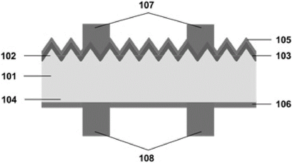
[0024] like figure 1 As shown, taking the p-type monocrystalline silicon substrate as an example, the double-sided crystalline silicon solar cell provided in this embodiment is provided with a front textured structure 102 on the front surface of the p-type monocrystalline silicon substrate 101, and the front surface is formed by phosphorus doping. The front pn emitter junction 103, the front passivation anti-reflection dielectric layer 105 and the front electrode 107, and the rear planar structure 104, the rear passivation anti-reflection dielectric layer 106 and the rear electrode 108 are sequentially arranged on the back of the p-type single crystal silicon substrate 101 , wherein, the back planar structure 104 is a planar p-type single crystal substrate formed directly on the silicon substrate and formed through a polishing process.
[0025] In this embodiment, the front passivation anti-reflection dielectric layer 105 is a silicon nitride film with a thickness of 70 to 80 ...
Embodiment 2
[0027] like figure 1 As shown, taking an n-type monocrystalline silicon substrate as an example, the double-sided crystalline silicon solar cell provided in this embodiment is provided with a front textured structure 102 on the front surface of an n-type monocrystalline silicon substrate 101, and the front boron doping is formed. The front pn emitter junction 103, the front passivation anti-reflection dielectric layer 105 and the front electrode 107, and the rear planar structure 104, the rear passivation anti-reflection dielectric layer 106 and the rear electrode 108 are sequentially arranged on the back of the p-type single crystal silicon substrate 101 , wherein, the back planar structure 104 is a planar n-type single crystal substrate formed directly on the silicon substrate and formed through a polishing process.
[0028] In this embodiment, the front passivation anti-reflection dielectric layer 105 is a double-layer film of aluminum oxide and silicon nitride, wherein the...
Embodiment 3
[0030] like figure 1 As shown, this embodiment is the situation when the preparation method of the double-sided crystalline silicon solar cell of the present invention is applied to p-type single crystal silicon, and specifically includes the following steps:
[0031] (1) Use an alkaline texturing solution containing potassium hydroxide and isopropanol at a temperature of 80°C to texturize the surface of the p-type single crystal silicon substrate 101 to form a front textured surface 102 and remove the silicon wafer at the same time cutting damage layer;
[0032] (2) Perform phosphorous doping to form the front emitter junction 103: phosphorous doping can be diffused in a tube furnace with a phosphorus oxychloride source, ion implantation or diffusion coated with a phosphorus-containing impurity layer, and the diffusion resistance is 40 to 200Ω / □ ;
[0033] (3) PECVD is used to deposit a process barrier layer of silicon oxide film on the front, with a thickness of 50 to 300n...
PUM
| Property | Measurement | Unit |
|---|---|---|
| Thickness | aaaaa | aaaaa |
| Thickness | aaaaa | aaaaa |
| Thickness | aaaaa | aaaaa |
Abstract
Description
Claims
Application Information
 - R&D
- Intellectual Property
- Life Sciences
- Materials
- Tech Scout
- Unparalleled Data Quality
- Higher Quality Content
- 60% Fewer Hallucinations
Browse by: Latest US Patents, China's latest patents, Technical Efficacy Thesaurus, Application Domain, Technology Topic, Popular Technical Reports.
© 2025 PatSnap. All rights reserved.Legal|Privacy policy|Modern Slavery Act Transparency Statement|Sitemap|About US| Contact US: help@patsnap.com