NiSe2 transition metal chalcogenide nanosheet as well as preparation method and application thereof
A technology of chalcogenides and transition metals, applied in the direction of metal selenide/telluride, chemical instruments and methods, binary selenium/tellurium compounds, etc., to achieve high catalytic efficiency and large specific surface area
- Summary
- Abstract
- Description
- Claims
- Application Information
AI Technical Summary
Problems solved by technology
Method used
Image

Examples
preparation example Construction
[0030] The present invention also provides the above-mentioned NiSe 2 A preparation method for transition metal chalcogenide nanosheets, comprising the following steps:
[0031] A) reacting the aqueous solution of the nickel source compound with ammonia water to obtain a reaction solution;
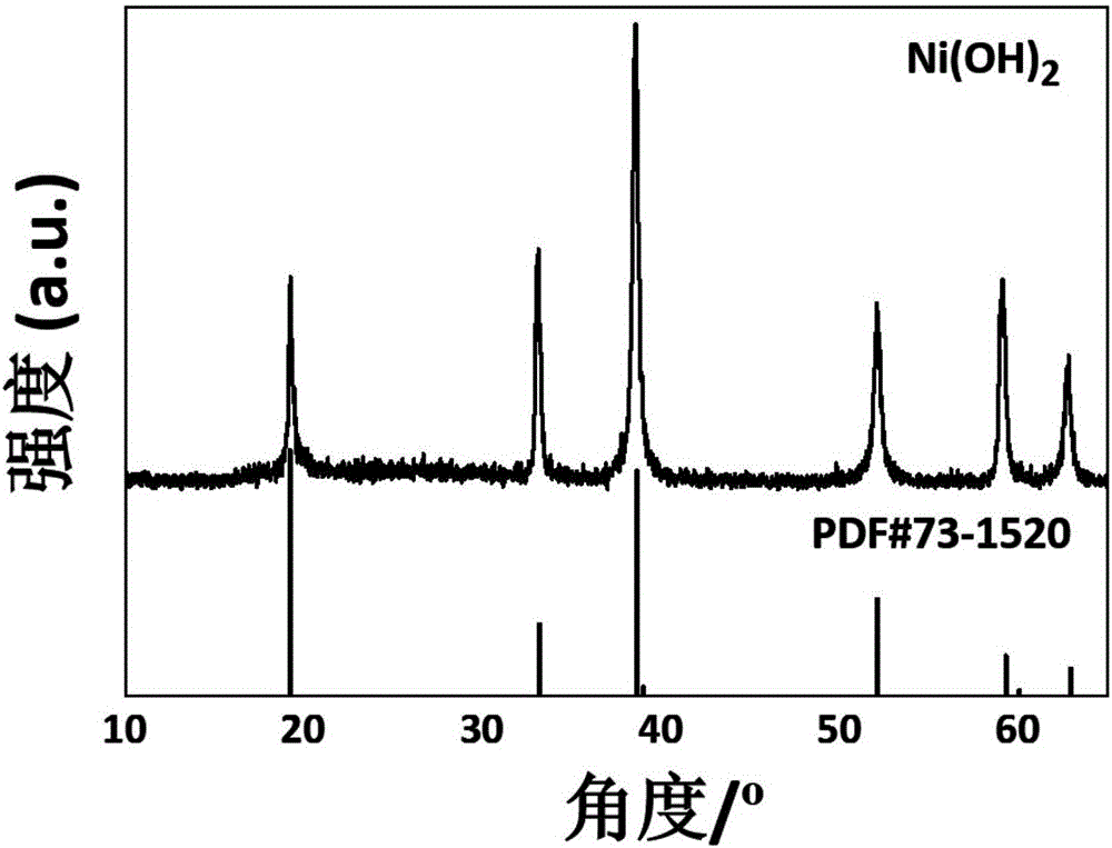
[0032] B) Insulating the substrate in the reaction solution obtained in step A) to obtain Ni(OH) grown on the surface 2 the substrate of the nanosheet;
[0033] C) Calcining the Se powder and the substrate obtained in step B) under the airflow of an inert atmosphere to obtain NiSe 2 Transition metal chalcogenide nanosheets.
[0034] The present invention uses nickel source compound and ammonia water as raw materials to prepare NiSe 2 Transition metal chalcogenide nanosheets.
[0035] The nickel source compound is preferably Ni(NO 3 ) 2 ·6H 2 O or NiCl 2 ·6H 2 O.
[0036] The nickel source compound is dissolved in water to obtain an aqueous solution, which is then reacted with am...
Embodiment 1
[0063] (1) Using nickel nitrate hexahydrate Ni(NO 3 ) 2 ·6H 2 O solid particle and ammonia solution are as the raw material of reaction, take the Ni (NO of 2.9079g) with analytical balance 3 ) 2 ·6H 2 O solid was dissolved in 10 mL of deionized water, and then 40 mL of ammonia water with a mass fraction of 25-28% was added dropwise, and magnetically stirred for half an hour to make it fully react.
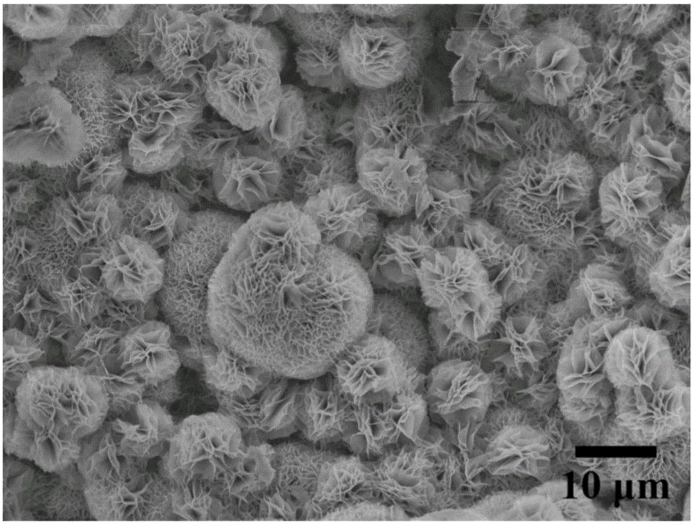
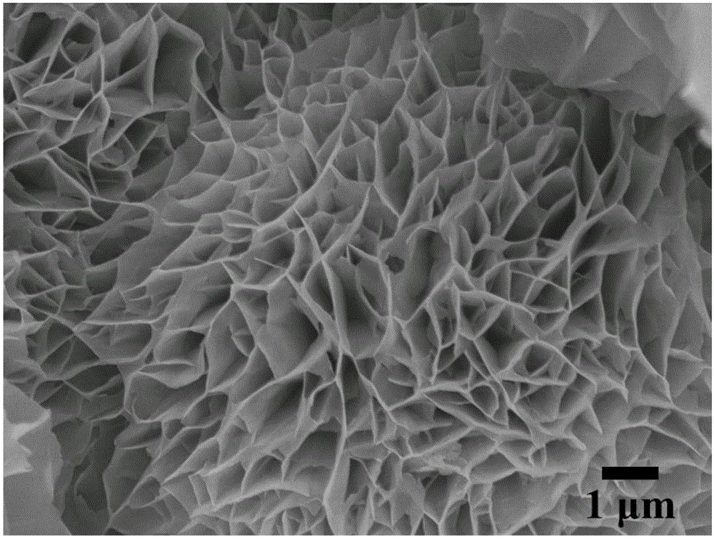
[0064] (2) Use acetone, absolute ethanol, and deionized water to ultrasonically clean the pure Si substrate produced by Suzhou Ruicai Semiconductor Co., Ltd. for 10 minutes, and then place the substrate in the center of a 100mL reactor with the polished side facing On; pour the above-mentioned stirred solution, cover it with a glass cover, put it into an electric oven and keep it warm at 90°C for 12 hours, and petal-shaped nanosheets grow on the surface of the substrate.
[0065] (3) After the reaction kettle was lowered to room temperature, the silicon chip was taken out, was...
PUM
| Property | Measurement | Unit |
|---|---|---|
| Length | aaaaa | aaaaa |
| Length | aaaaa | aaaaa |
Abstract
Description
Claims
Application Information
 - Generate Ideas
- Intellectual Property
- Life Sciences
- Materials
- Tech Scout
- Unparalleled Data Quality
- Higher Quality Content
- 60% Fewer Hallucinations
Browse by: Latest US Patents, China's latest patents, Technical Efficacy Thesaurus, Application Domain, Technology Topic, Popular Technical Reports.
© 2025 PatSnap. All rights reserved.Legal|Privacy policy|Modern Slavery Act Transparency Statement|Sitemap|About US| Contact US: help@patsnap.com