High-breakdown-voltage gallium-oxide Schottky diode and manufacturing method thereof

A Schottky diode, high breakdown voltage technology, used in circuits, electrical components, semiconductor/solid-state device manufacturing, etc. and other problems, to achieve the effect of enhanced depletion, good device performance, and improved breakdown voltage

Active Publication Date: 2017-06-20
XIDIAN UNIV
View PDF8 Cites 31 Cited by
  • Summary
  • Abstract
  • Description
  • Claims
  • Application Information

AI Technical Summary

Problems solved by technology

Pn junction diodes and Schottky diodes (SBD) are the two most commonly used devices. Compared with pn junction diodes, Schottky diodes have the advantages of high frequency, small forward voltage drop and short reverse recovery time. Advantages, but the breakdown voltage of the Schottky diode depends largely on the strong electric field at the edge caused by the junction curvature, so the breakdown voltage of the Schottky diode is much smaller than the ideal value, so in ...

Method used


Image

  • High-breakdown-voltage gallium-oxide Schottky diode and manufacturing method thereof
  • High-breakdown-voltage gallium-oxide Schottky diode and manufacturing method thereof

Examples


Embodiment 1

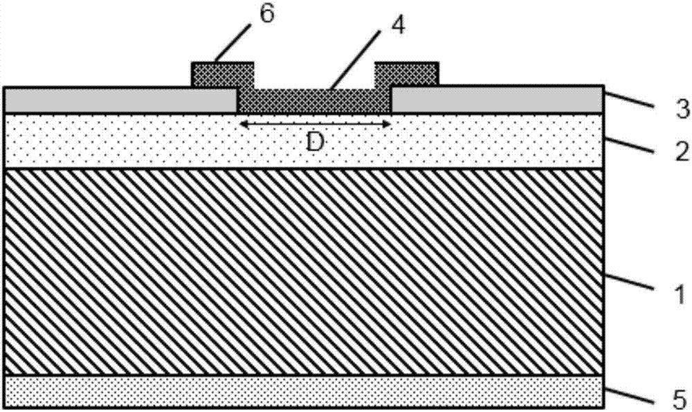
[0030] Example 1, fabricate a Schottky diode with a thickness of 300nm as the organic ferrodielectric and using vinylidene fluoride-trifluoroethylene copolymer P(VDF-TrFE) as the organic ferrodielectric.

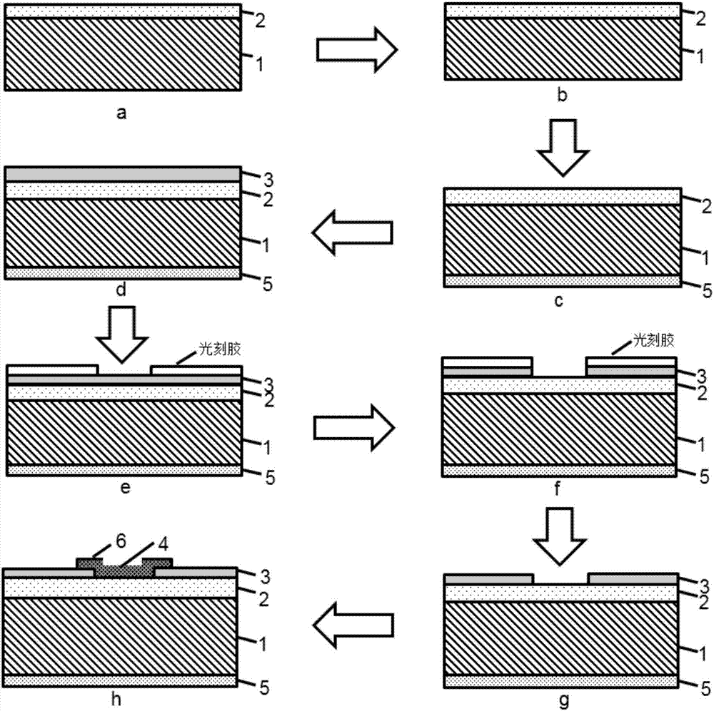
[0031] Step 1, for the carrier concentration already at 10 18 cm -3 Epitaxially grown on the substrate with a carrier concentration of 10 16 cm -3 Ga 2 o 3 The epitaxial layer samples were cleaned as figure 2 a.

[0032] Ga 2 o 3 The samples were cleaned organically, that is, put them into an acetone solution for 5 minutes, then put them into an ethanol solution for 5 minutes; then wash them with deionized water; then put them into HF:H 2 Corrosion was carried out in the solution of O=1:1 for 50s; finally, it was washed with flowing deionized water and dried with high-purity nitrogen.

[0033] Step 2, etch, such as figure 2 b.

[0034] Put the cleaned sample face down into the ICP etching reaction chamber, and etch the lower surface of the substrate. The process...

Embodiment 2

[0048] Example 2, making a Schottky diode with a thickness of 400nm as the organic ferrodielectric, and Ag-P (VDF-TrFE) material doped with silver nanoparticles as the organic ferrodielectric.

[0049] Step 1, for the carrier concentration already at 10 19 cm -3 Epitaxially grown on the substrate with a carrier concentration of 10 15 cm -3 Ga 2 o 3 The epitaxial layer samples were cleaned as figure 2 a.

[0050] The specific implementation of this step is the same as step 1 of Embodiment 1.

[0051] Step two, etching.

[0052] Put the cleaned sample face down into the ICP etching reaction chamber, and etch the lower surface of the substrate. The process conditions are: the power of the upper electrode is 100W, the power of the lower electrode is 10W, the pressure of the reaction chamber is 25Pa, BCl 3 The flow rate of Ar gas is 10 sccm, the flow rate of Ar gas is 20 sccm, and the etching time is 5 min.

[0053] Step 3, preparing the cathode electrode.

[0054] Put t...

Embodiment 3

[0067] Example 3, fabricating a Schottky diode with an organic ferrodielectric thickness of 450 nm and a ZnS-P (VDF-TrFE) material doped with zinc sulfide nanoparticles as the organic ferrodielectric.

[0068] Step A, for a carrier concentration already at 10 19 cm -3 Epitaxially grown on the substrate with a carrier concentration of 10 15 cm -3 Ga 2 o 3 The epitaxial layer samples were cleaned.

[0069] The specific implementation of this step is the same as step 1 of Embodiment 1.

[0070] Step B, put the cleaned sample face down into the ICP etching reaction chamber, and etch the lower surface of the substrate. The process conditions are: the power of the upper electrode is 100W, the power of the lower electrode is 10W, and the pressure of the reaction chamber is 30Pa , BCl 3 The flow rate of Ar gas is 10 sccm, the flow rate of Ar gas is 20 sccm, and the etching time is 5 min.

[0071] Step C, put the etched sample face down into the electron beam evaporation table to...


PUM

PropertyMeasurementUnit
Thicknessaaaaaaaaaa
Carrier concentrationaaaaaaaaaa
Thicknessaaaaaaaaaa

Abstract

The invention discloses a high-breakdown-voltage gallium-oxide Schottky diode structure comprising a highly-doped n type Ga2O3 substrate (1), a lowly-doped n type Ga2O3 epitaxial layer (2), and an anode electrode (4). A cathode electrode (5) is deposited at the lower surface of the substrate; the anode electrode and the epitaxial layer (2) are in Schottky contact; and the cathode electrode and the substrate (1) are in ohmic contact. An organic ferroelectric dielectric layer (3) with a thickness of 300 to 500 nm is deposited on the upper surface of the epitaxial layer (2). A circular hole is etched in the organic ferroelectric dielectric layer; the anode electrode is deposited in the hole of the organic ferroelectric dielectric layer; a field plate (6) is deposited at the edge of the hole; and the field is arranged on the organic ferroelectric dielectric layer and is connected with the anode electrode. Therefore, the reverse breakdown voltage can be improved and the forward characteristic is not changed. The high-breakdown-voltage gallium-oxide Schottky diode can be applied to a high-speed integration circuit and a microwave circuit.

Description

technical field [0001] The invention belongs to the technical field of semiconductor devices, in particular to a Schottky diode device structure and manufacturing method, which can be used in high-speed integrated circuits and microwave technologies. Background technique [0002] Ga 2 o 3 As a newly developed wide bandgap semiconductor material, semiconductor materials have aroused widespread interest due to their large bandgap, high breakdown field strength, and small on-resistance. Because of their relatively large bandgap, they can be prepared High-power devices and high-voltage switching devices, and the higher mobility also ensures that the device has a higher response speed. Therefore based on Ga 2 o 3 The power electronic devices of materials have very broad military and civilian prospects. In 2015, Kohei Sasaki et al. used a field plate structure to realize a Schottky diode with a breakdown voltage of 920V. Refer to Kohei Sasaki, Masataka Higashiwaki, Ken Goto e...

Claims


Application Information

Patent Timeline
IPC IPC(8): H01L29/872H01L21/329
Inventor 冯倩李翔韩根全黄璐方立伟邢翔宇张进成郝跃
Owner XIDIAN UNIV
Why Eureka
Try Eureka