Electromagnetic field near-field imaging system and method based on pulsed light detection magnetic resonance

A near-field imaging and magnetic resonance technology, which is applied in the fields of electromagnetic field characteristics, analysis by nuclear magnetic resonance, fluorescence/phosphorescence, etc., can solve the problems of unclear near-field distribution characteristics of the electromagnetic field inside the device, unsatisfactory requirements, and limited scanning accuracy.

Inactive Publication Date: 2017-11-17
南京昆腾科技有限公司
View PDF6 Cites 65 Cited by
  • Summary
  • Abstract
  • Description
  • Claims
  • Application Information

AI Technical Summary

Problems solved by technology

[0006] The above-mentioned currently popular methods mainly have the following problems: 1. Software simulation and numerical calculation methods In the case of simulating microwave and millimeter-wave high-frequency and high-integration chips, due to the complexity of the near-field of the electromagnetic field, the software simulation cannot avoid certain distortions
2. Using a traditional black box network analyzer to measure the S-parameters of microwave and millimeter wave devices can only measure the external characteristics of the device, and cannot explain the near-field distribution characteristics of the internal electromagnetic field of the device
3. Using a field strength meter with a special high-frequency antenna to scan the surface of microwave and millimeter-wave devices, because the size of the special high-frequency antenna itself is often relatively large, the scanning accuracy is limited; in addition, the special high-frequency antenna itself is Made of metal, the antenna itself disturbs the electromagnetic field, and the measured field is inaccurate
[0007] Under the above technical background, for the near-field electromagnetic field imaging scene on the surface of microwave and millimeter-wave chips, the existing microwave near-field imaging analysis methods do not meet the requirements
Therefore, for the near-field electromagnetic field imaging scene on the surface of microwave and millimeter-wave chips, the existing microwave near-field imaging analysis methods do not meet the requirements.

Method used


Image

  • Electromagnetic field near-field imaging system and method based on pulsed light detection magnetic resonance
  • Electromagnetic field near-field imaging system and method based on pulsed light detection magnetic resonance
  • Electromagnetic field near-field imaging system and method based on pulsed light detection magnetic resonance

Examples


Embodiment 1

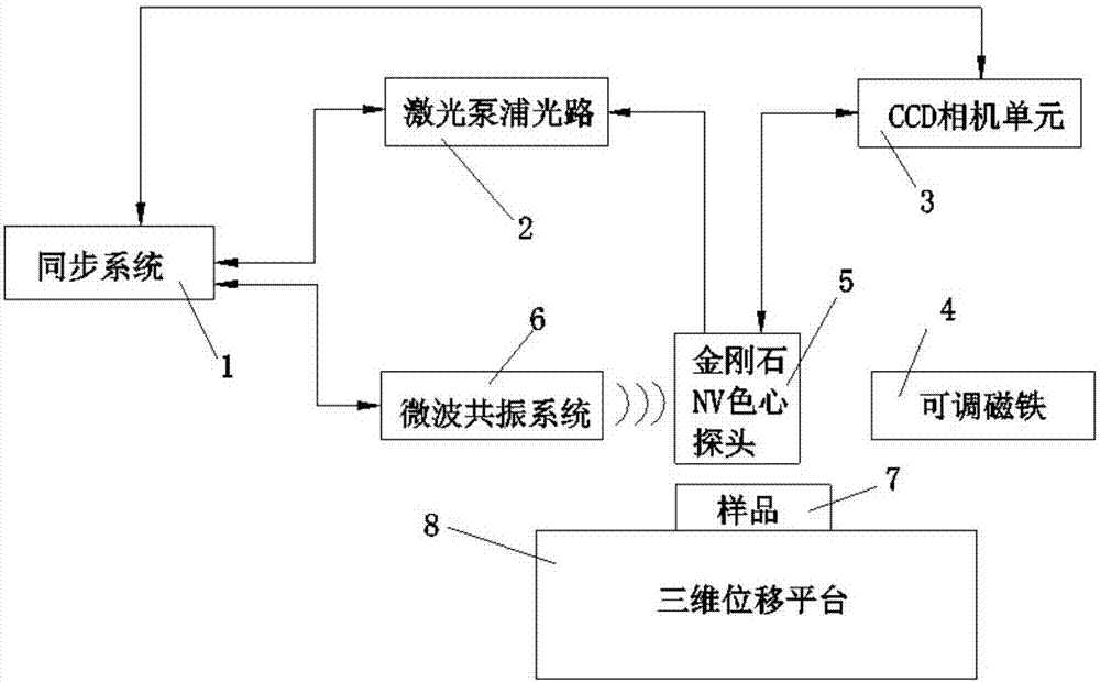
[0108] According to the present invention, assuming that the system measures the microwave field on a microwave chip, the specific implementation method of this embodiment using the present invention to realize the microwave field measurement and imaging is as follows:

[0109]1. First debug the system, set the laser intensity to about 15 milliwatts, the microwave intensity to 0dbm, and the microwave scanning frequency range to 2500MHz-3300MHz.

[0110] 2. Set the CCD exposure time to 17980 microseconds, the frame rate to 63, the gain to 1, the trigger mode to external hardware trigger, and each trigger captures 1 frame.

[0111] 3. Set the timing of the TTL signal of the synchronization system, initialize the laser for about 300ns, microwave pulse for about 50ns, and the interval between the laser Readout pulse and the initialization laser pulse is 3 microseconds.

[0112] 4. Place the microwave chip under the NV color center probe, the microwave chip should be as close as po...

Embodiment 2

[0122] According to the present invention, assuming that the system performs diagnostic measurement of electromagnetic compatibility problems on a microwave chip, the specific implementation method of this embodiment using the present invention to realize the diagnostic measurement of electromagnetic compatibility of microwave chips is as follows:

[0123] 1. Analyze the image of the microwave field on the surface of the microwave chip. Different wires inside the microwave chip are equivalent to a microwave waveguide, and each microwave wire is equivalent to an antenna; first cut off a part of the microwave waveguide B signal, and only keep it for measurement Radiation disturbs the signal emitted by the microwave waveguide A.

[0124] 2. Repeat steps 1 to 11 in Device Example 1. The image of the disturbance electromagnetic field generated by microwave waveguide A at microwave waveguide B can be obtained. According to the image, the degree of influence of microwave waveguide A...

Embodiment 3

[0128] According to the present invention, assuming that the system performs characteristic measurement of the electromagnetic field distribution in the microwave resonator, the specific implementation method of this embodiment using the present invention to realize the characteristic measurement of the electromagnetic field distribution in the microwave resonator is as follows:

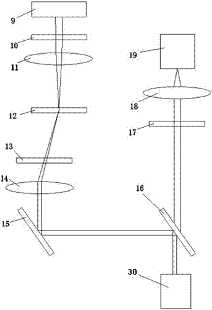
[0129] 1. Replace the diamond probe of the system with a single-mode optical fiber. One end of the optical fiber is glued with diamond, and the other end is placed under the focus of the probe objective lens 30. The probe objective lens 30 focuses the pump laser light on the single-mode optical fiber, and then strikes the laser light on the diamond through the optical fiber, and the fluorescence emitted by the diamond can also be collected by the objective lens 30 through the optical fiber.

[0130] 2. Insert the diamond fiber probe into the microwave resonant cavity.

[0131] 3. Repeat steps 1 to 9 ...


PUM

PropertyMeasurementUnit
wavelengthaaaaaaaaaa

Abstract

The invention discloses an electromagnetic field near-field imaging system and method based on pulsed light detection magnetic resonance. The system consists of a laser pump optical path, a microwave source, a diamond NV color-center probe, a CCD camera unit, a synchronization system, a displacement scanning platform, control software and a data analysis imaging system. In the system, a large diamond single crystal containing the NV color-center is used as a detection unit, a static magnetic field is used to split a magnetic resonance peak of the diamond NV color-center into eight peaks, the eight resonance peaks correspond to four crystal axis directions <111>, <1-11>, <-111>, <11-1> of a diamond lattice structure, by measuring the Rabi frequency of each resonance peak, the strength of a circularly polarized microwave field perpendicular to the corresponding crystal axis direction is obtained, and through comprehensive calculation of the microwave field strengths in the four directions, the strength and direction of a microwave vector are then reconstructed. Through the microwave near-field high-resolution imaging of a local region of a microwave chip under measurement, the quantitative data can be provided for the failure analysis of the chip.

Description

technical field [0001] The invention belongs to the field of electromagnetic near-field imaging, and relates to an electromagnetic near-field imaging system and method. Background technique [0002] With the continuous development of microwave radio frequency technology, microwave and millimeter wave technology has become a hot technology in 5G communication, automatic driving, military aerospace, consumer electronics and other aspects due to its advantages of high bandwidth, miniaturization, and high integration. Millimeter-wave near-field imaging technology has broad applications in high-resolution target recognition and gesture detection and interaction. The detection and imaging of the near-field distribution of the surface electromagnetic field of microwave and millimeter wave devices is of great significance for the promotion and application of microwave and millimeter wave technology. For a long time, in the field of microwave and radio frequency, there is still a la...

Claims


Application Information

Patent Timeline
Patent Type & Authority Applications(China)
IPC IPC(8): G01R29/08G01N21/64G01N24/08
CPCG01N21/64G01N24/08G01R29/08
Inventor 杜关祥杨博胡振忠余彦路王永进
Owner 南京昆腾科技有限公司
Why Eureka
Try Eureka