A kind of preparation method of silicon germanium black phosphorene pin heterojunction solar cell

A technology of solar cells and black phosphorene, which is applied in the field of solar cells, can solve problems such as living environment disasters, greenhouse effects, and environmental pollution, and achieve the effects of simple preparation methods, improved absorption efficiency, and improved photoelectric conversion efficiency

Active Publication Date: 2019-02-01
厦门鸾创科技有限公司
View PDF6 Cites 0 Cited by
  • Summary
  • Abstract
  • Description
  • Claims
  • Application Information

AI Technical Summary

Problems solved by technology

At the same time, the use of fossil fuels releases a large amount of toxic gas and carbon dioxide gas, causing serious environmental pollution and greenhouse effect, and causing unprecedented disasters to the living environment of human beings.

Method used


Image

  • A kind of preparation method of silicon germanium black phosphorene pin heterojunction solar cell
  • A kind of preparation method of silicon germanium black phosphorene pin heterojunction solar cell
  • A kind of preparation method of silicon germanium black phosphorene pin heterojunction solar cell

Examples


preparation example Construction

[0016] see Figure 1-6 , the present invention firstly provides a method for preparing a silicon germanium black phosphorene PIN heterojunction solar cell, specifically comprising the following steps:

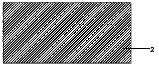
[0017] see figure 1 , providing an N-type silicon substrate 2, and cleaning the N-type silicon substrate 2;

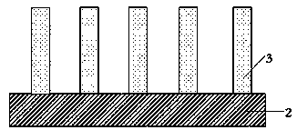
[0018] see figure 2 , using dry etching or wet etching to prepare an N-type silicon nanowire array 3 in the N-type silicon substrate 2 .

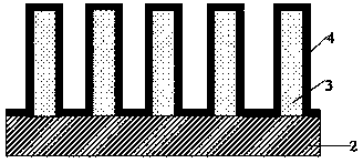
[0019] see image 3 , using the PECVD method to deposit an intrinsic amorphous germanium layer 4 with a thickness of 20-100 nanometers on the N-type silicon nanowire array 3;

[0020] see Figure 4 , using a liquid phase stripping method to form a solution containing black phosphorene, and spin-coating the solution containing black phosphorene on the intrinsic amorphous germanium layer 5 to obtain a P-type black phosphorene layer 5 with a thickness of 20-150 nanometers;

[0021] see Figure 5 , forming indium tin oxide or alu...

Embodiment 1

[0024] A method for preparing a silicon-germanium black phosphorene PIN heterojunction solar cell, specifically comprising the following steps:

[0025] First, the N-type silicon substrate was ultrasonically cleaned in acetone, ethanol, and deionized water for 20 minutes; 2 SO 4 :H 2 o 2 The mixed solution was heated to 110° C. for 1 hour, then rinsed with deionized water and dried with a nitrogen gun, and set aside.

[0026] Next, immerse the N-type silicon substrate in an aqueous solution containing 4.8M hydrofluoric acid and 0.02M silver nitrate, react at room temperature for 20-50 minutes, take out the etched N-type silicon substrate, and clean it to obtain an N-type silicon substrate. In the silicon nanowire array, by controlling the reaction time, the length of a single silicon nanowire in the N-type silicon nanowire array is 0.5-1 micron, the diameter of the single silicon nanowire is 50-100 nanometers, and the diameter of the adjacent silicon nanowire is The pitch ...


PUM

PropertyMeasurementUnit
thicknessaaaaaaaaaa
thicknessaaaaaaaaaa
thicknessaaaaaaaaaa

Abstract

The invention provides a preparation method for a silicon-germanium black phosphorus alkene PIN heterojunction solar cell. The method comprises the steps: washing an N-type silicon substrate, preparing an N-type silicon nanowire array in the N-type silicon substrate, sequentially forming an intrinsic amorphous germanium layer, a P-type black phosphorus alkene layer and a transparent conductive layer, finally forming a back electrode on the back surface of the N-type silicon substrate and forming an upper electrode on the transparent conductive layer. The preparation method is simple, and the setting of the silicon nanowire array improves the sunlight absorption efficiency of the solar cell. The black phosphorus alkene serves as the novel two-dimensional semiconductor material, and forms a PIN heterojunction with the N-type silicon nanowire array and the intrinsic amorphous germanium layer. The PIN heterojunction can achieve the effective photoelectric conversion. Moreover, the setting of a radial structure facilitates the separation and transmission of electronic hole pairs, and further improves the photoelectric conversion efficiency of the solar cell.

Description

technical field [0001] The invention relates to the technical field of solar cells, in particular to a method for preparing a silicon-germanium black phosphorene PIN heterojunction solar cell. Background technique [0002] Since the industrial revolution, with the development and progress of industrialization, the demand for energy has also increased sharply, among which fossil fuels are the most important energy materials. However, the total reserves of fossil fuel energy on the earth are limited, and they are non-renewable energy sources, so the world is facing a severe energy situation. At the same time, the use of fossil fuels releases a large amount of toxic gas and carbon dioxide gas, causing serious environmental pollution and greenhouse effect, and causing unprecedented disasters to the living environment of human beings. People have been strongly aware of the seriousness of the negative impact of the use of fossil fuels. Therefore, the proposal of "changing the en...

Claims


Application Information

Patent Timeline
Patent Type & Authority Patents(China)
IPC IPC(8): H01L31/20H01L31/028H01L31/075B82Y40/00
CPCB82Y40/00H01L31/028H01L31/075H01L31/202Y02E10/547Y02E10/548Y02P70/50
Inventor 刘辉刘聪贤朱眉清
Owner 厦门鸾创科技有限公司
Why Eureka
Try Eureka