Crystal material, preparation method thereof and application as laser crystal
A crystal material, single crystal technology, applied in the direction of polycrystalline material growth, laser, crystal growth, etc., can solve the problems of unfavorable crystal pumped laser performance, self-final state bottleneck effect, low LD pumping efficiency, etc. State bottleneck effect, reduction of lifetime and particle number, effect of high mechanical strength
- Summary
- Abstract
- Description
- Claims
- Application Information
AI Technical Summary
Problems solved by technology
Method used
Image
Examples
Embodiment 1
[0050] The preparation of embodiment 1 crystal material sample
[0051] Weigh CaCO according to the ratio in the following chemical reaction formula 3 , La 2 o 3 , Ga 2 o 3 、Er 2 o 3 and Nd 2 o 3 , mix well to get the raw material:
[0052] 2CaCO 3 +(1-x-y)La 2 o 3 +3Ga 2 o 3 +yEr 2 o 3 +xNd 2 o 3 →2CaNd x Er y La (1-x-y) Ga 3 o 7 +2CO 2 ↑
[0053] Press the raw material into a sheet, put it into a platinum crucible, put it into an ordinary sintering furnace, slowly raise the temperature to the pre-sintering temperature at a certain rate, and keep it for a period of time; Sample: Repeat the above pre-sintering and sintering steps until the X-ray powder diffraction is completely consistent with the XRD standard JCPDS card of the CLGO crystal to obtain a polycrystalline sample of the crystalline material.
[0054] Put the raw materials into the iridium crucible of Ф62mm×40mm. In order to avoid the oxidation of the iridium crucible, firstly extract the ai...
Embodiment 2
[0058] The optical property measurement of embodiment 2 gained sample
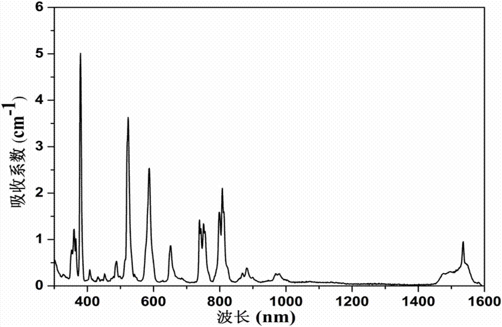
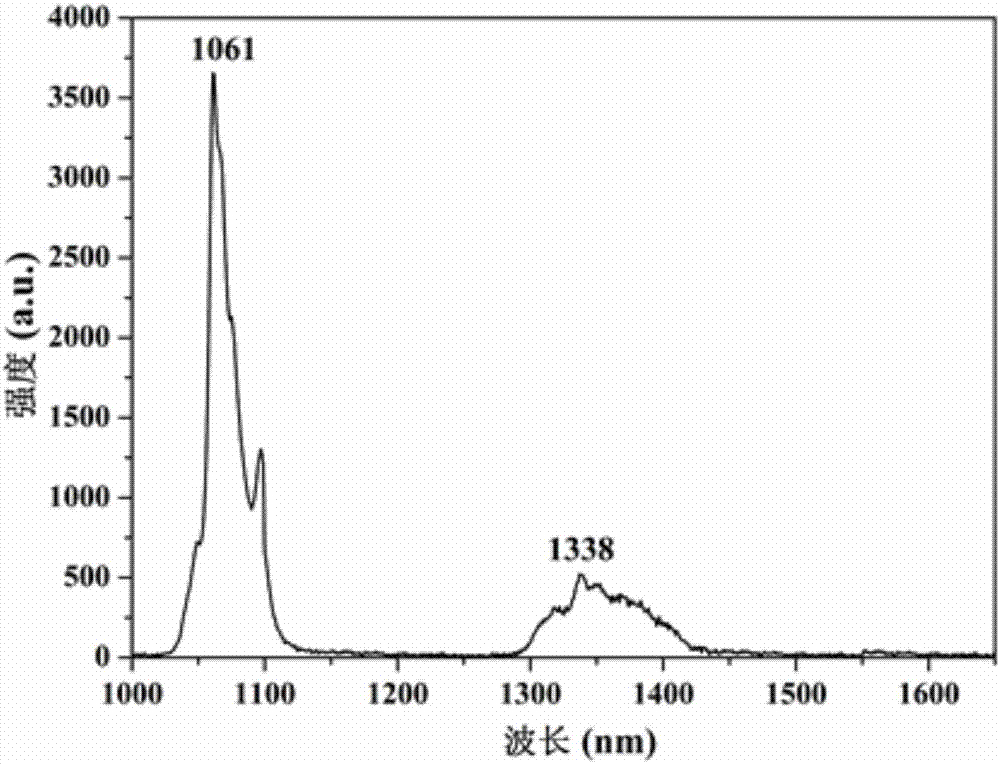
[0059] Take sample S1 separately # ~S5 # , the processed size is 5.0×5.0×1.0mm 3 The crystal slices were tested for spectral properties.
[0060] The results showed that sample S1 # ~S5 # The absorption spectrum also shows the Nd 3+ and Er 3+ The characteristic absorption peaks, wherein, the peak wavelengths are 378,488,523,652,801,979 and 1536nm respectively, corresponding to Er: 4 I 15 / 2 arrive 4 G 11 / 2 + 2 K 15 / 2 , 4 f 7 / 2 , 2 h 11 / 2 , 4 f 9 / 2 , 4 I 9 / 2 , 4 I 11 / 2 and 4 I 13 / 2 transition, and the absorption peaks with peak wavelengths of 360, 588, 750, 808, and 882nm respectively correspond to Nd 3+ : 4 I 9 / 2 arrive 4 D. 3 / 2 , 4 G 5 / 2 + 2 G 7 / 2 , 4 f 7 / 2 + 4 S 3 / 2 , 4 f 5 / 2 + 2 h 9 / 2 and 4 f 3 / 2transition, the absorption peak with the largest absorption intensity and the widest width is located in the 780-835nm band, and the peak wavelength is 808nm, mainly from...
Embodiment 3
[0065] The application of embodiment 3 gained sample in laser device
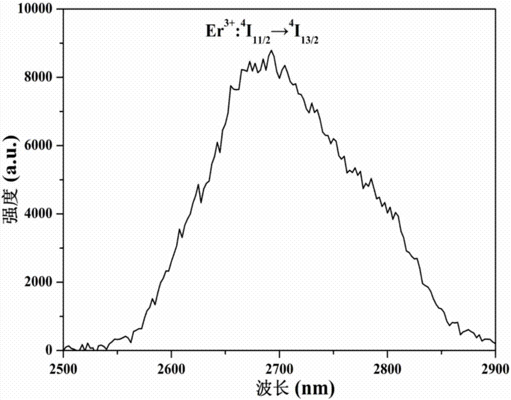
[0066] Take sample S1 separately # ~S5 # , the processed size is 2mm×2mm×(5~10)mm, the two ends of the crystal are 2mm×2mm polished, and it is applied to the laser device. The device diagram of the laser device is shown in Figure 4 As shown, the crystal sample is put into a water-sealed copper tube, the pump source used is 808nm LD, and the end-pump mode is adopted. The input mirror is a concave mirror with a diameter of 200mm, which is highly transparent at 808nm and highly reflective at 2.7μm. The coupling mirror is a flat mirror with transmittance of 1%, 2% and 3% at the laser wavelength. The laser spectrum is measured by a laser wavelength meter, the model is 821B-IR, Bristol, and the laser power is measured by a power meter, the model is LPE-1B.
[0067] The results showed that the samples S1 were applied respectively # ~S5 # The laser devices are capable of achieving 2.7μm band mid-infrared ult...
PUM
| Property | Measurement | Unit |
|---|---|---|
| wavelength | aaaaa | aaaaa |
| size | aaaaa | aaaaa |
| size | aaaaa | aaaaa |
Abstract
Description
Claims
Application Information


