

A manufacturing method of an economical high-precision surface-enhanced Raman active substrate
A surface-enhanced Raman and active substrate technology, which is applied in the field of physical and chemical detection, can solve the problems of Raman signal enhancement, enhancement effect, and repeatability. The effect of industrial production
- Summary
- Abstract
- Description
- Claims
- Application Information
AI Technical Summary
Problems solved by technology
Method used
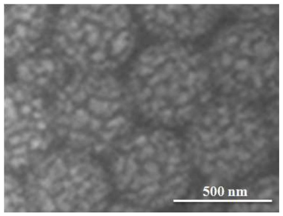
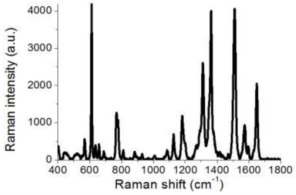
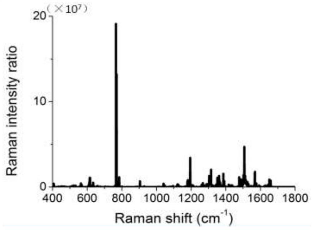
Image

Examples
Embodiment 1
[0036] A method for manufacturing an economical high-precision surface-enhanced Raman active substrate, comprising the following steps:
[0037] 1) Initial preparation
[0038]① Raw material preparation: Prepare tetraethyl orthosilicate, absolute ethanol, ammonia water, several silicon wafers, nano-gold materials for magnetron sputtering, cetyltrimethylammonium bromide;
[0039] ② Preparation of tooling and auxiliary materials: Prepare four glass containers, magnetic stirrer, stirring equipment, deionized water, and select a hydrophobic pad with a thickness of 1mm and a size error of less than 1‰;
[0040] ③ Production equipment preparation: prepare ultrasonic generating equipment, magnetron sputtering equipment, oven;
[0041] ④ Detection equipment preparation: rhodamine solution, Raman signal laser detector;
[0042] 2) Preparation of silica microsphere suspension
[0043] ① Mix tetraethyl orthosilicate and absolute ethanol at a volume ratio of 1:4, stir evenly, and then ...
Embodiment 2
[0061] A method for manufacturing an economical high-precision surface-enhanced Raman active substrate is basically the same as in Example 1, the difference being:
[0062] 2) Preparation of silica microsphere suspension
[0063] ①Mix tetraethyl orthosilicate and absolute ethanol at a volume ratio of 1:3.5;
[0064] ② Mix ammonia water and absolute ethanol at a volume ratio of 1:4;
[0065] ③ Evenly drop the mixed liquid in the first glass container into the second glass container at a dropping speed of 1.5 drops / second, start the stirring device at the same time, keep the liquid in the second glass container at a stirring speed of 500r / min, and the dropping process is completed Then continue to stir for 1.5h to obtain the ready-to-use mixed solution;
[0066] ④ Evenly drop tetraethyl orthosilicate with a volume of 70% of the total solution volume into the ready-to-use mixed solution obtained in step ③ at a dropping speed of 1.5 drops / second, and keep the liquid in the secon...
Embodiment 3
[0077] A method for manufacturing an economical high-precision surface-enhanced Raman active substrate is basically the same as in Example 1, the difference being:
[0078] 2) Preparation of silica microsphere suspension
[0079] ①Mix tetraethyl orthosilicate and absolute ethanol at a volume ratio of 1:5;
[0080] ② Mix ammonia water and absolute ethanol at a volume ratio of 1:5.5;
[0081] ③ Evenly drop the mixed solution in the first glass container into the second glass container at a rate of 0.5 drops / second;
[0082] 4. Evenly drop tetraethyl orthosilicate with a volume of 75% of the total solution volume in the ready-to-use mixed solution obtained in step 3. at a dropping speed of 0.5 drops / second;
[0083] 6. Mixing the silicon dioxide microspheres prepared in step 5. with deionized water in a mass ratio of 1:20;
[0084] 3) Preparation of Surface Array Ordered Monolayer Silica Surface Activation Matrix
[0085] ①Add 0.1g of cetyltrimethylammonium bromide to the fou...
PUM
| Property | Measurement | Unit |
|---|---|---|
| diameter | aaaaa | aaaaa |
| thickness | aaaaa | aaaaa |
| thickness | aaaaa | aaaaa |
Abstract
Description
Claims
Application Information