

Formaldehyde sensor based on organic field effect transistor
A formaldehyde sensor and organic field technology, applied in the field of sensors, can solve the problems of pollution, poor flexibility of formaldehyde sensors, high detection limit of formaldehyde sensors, etc., and achieve the effect of solving secondary pollution, excellent water absorption characteristics, and easy industrialized large-scale production
- Summary
- Abstract
- Description
- Claims
- Application Information
AI Technical Summary
Problems solved by technology
Method used
Image

Examples
preparation example Construction
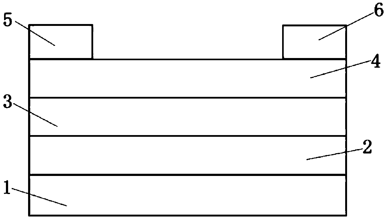
[0036] The preparation method of the organic semiconductor layer can be a method in plasma-enhanced chemical vapor deposition, thermal oxidation, spin coating, vacuum evaporation, drop film, embossing, printing or air spray; the thickness of the organic semiconductor layer 4 is 50 ~120nm.
[0037] The materials of the gate electrode, source electrode and drain electrode are all one or more of graphene, carbon nanotubes, metal element nanowires, zinc oxide, titanium oxide, indium tin oxide or polymer electrode materials. The preparation method It can be one of various deposition methods such as vacuum thermal evaporation, magnetron sputtering, plasma-enhanced chemical vapor deposition, screen printing, printing, and spin coating. The thickness of the gate electrode, the source electrode and the drain electrode are all 50-80nm.
[0038] The metal nanowires are iron nanowires, copper nanowires, silver nanowires, gold nanowires, aluminum nanowires, nickel nanowires, cobalt nanowi...
Embodiment 1
[0052] The preparation method is as follows:
[0053] ① Thoroughly clean the PI substrate sputtered with 50nm ITO as the gate electrode, and dry it with dry nitrogen after cleaning;
[0054] ② Prepare a PS film on ITO by spin coating to form a gate insulating layer of 100nm;
[0055] ③The spin-coated PS film is heated and baked;
[0056] 4. Spin-coat indigo on the grid insulating layer: diatom mud mass ratio is 100nm of the organic semiconductor layer of 97:3;
[0057] ⑤ Vacuum evaporation is used to prepare 80nm copper source electrodes and drain electrodes.
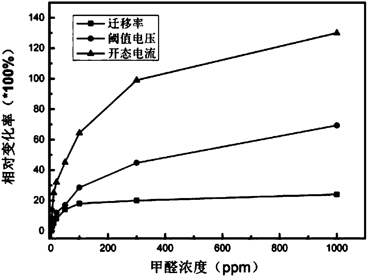
[0058] The formaldehyde response characteristics of the device are tested, and the saturation current I of the device is measured SD =6μA, carrier mobility μ=2×10 -3 cm 2 / Vs, threshold voltage V TH =-14V, good response to formaldehyde at room temperature.
Embodiment 2
[0060] The preparation method is as follows:
[0061] ① Thoroughly clean the PEI substrate sprayed with 80nm silver nanowires as the gate electrode, and dry it with dry nitrogen after cleaning;
[0062] ② Prepare a PMMA film on the silver nanowire by spin coating method to form a gate insulating layer of 520nm;
[0063] ③Heating and baking the spin-coated PMMA film;
[0064] 4. Spin-coat indigo on the grid insulating layer: diatom mud mass ratio is 120nm of the organic semiconductor layer of 94:6;
[0065] ⑥A silver source electrode and a drain electrode of 70nm were prepared by vacuum evaporation.
[0066] The formaldehyde response characteristics of the device are tested, and the saturation current I of the device is measured SD =12μA, carrier mobility μ=0.004cm 2 / Vs, threshold voltage V TH =-16V, good response to formaldehyde at room temperature.
PUM
| Property | Measurement | Unit |
|---|---|---|
| Thickness | aaaaa | aaaaa |
| Thickness | aaaaa | aaaaa |
| Thickness | aaaaa | aaaaa |
Abstract
Description
Claims
Application Information