Charge storage-type insulated gate bipolar transistor with trench gate and manufacturing method of charge storage-type insulated gate bipolar transistor

A bipolar transistor and charge storage technology, applied in semiconductor/solid-state device manufacturing, circuits, electrical components, etc., can solve problems such as the deterioration of the short-circuit safe working area of ​​the device, increasing the saturation current density of the device, and reducing the switching speed of the device, etc. Achieve the effect of improving forward conduction performance and improving overall performance

Active Publication Date: 2018-01-23
UNIV OF ELECTRONIC SCI & TECH OF CHINA
View PDF5 Cites 29 Cited by
  • Summary
  • Abstract
  • Description
  • Claims
  • Application Information

AI Technical Summary

Problems solved by technology

[0005] The implementation of method (1) will increase the gate-emitter capacitance and gate-collector capacitance at the same time, and the switching process of the IGBT is essentially the process of charging/discharging the gate capacitance, so the increase in the gate capacitance will Makes the charging/discharging time longer, which in turn causes the switching speed to decrease
Therefore, the deep trench gate depth will reduce the switching speed of the device, increase the switching loss of the device, and affect the compromise characteristics of the device's conduction voltage drop and switching loss; and the implementation of method (2) will increase the device's switching loss The gate capacitance will reduce the switching speed of the device and increase the switching loss, which will affect the compromise between the condu

Method used


Image

  • Charge storage-type insulated gate bipolar transistor with trench gate and manufacturing method of charge storage-type insulated gate bipolar transistor
  • Charge storage-type insulated gate bipolar transistor with trench gate and manufacturing method of charge storage-type insulated gate bipolar transistor
  • Charge storage-type insulated gate bipolar transistor with trench gate and manufacturing method of charge storage-type insulated gate bipolar transistor

Examples


Embodiment 1

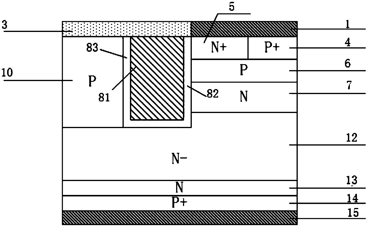
[0066] This example proposes as figure 2 The shown trench gate charge storage type insulated gate bipolar transistor includes: a P-type collector region 14, a collector metal 15 located on the back of the P-type collector region 14, and a The N-type electric field stop layer 13 and the N-type drift region 12 located above the N-type electric field stop layer 13; it is characterized in that: the N-type drift region 12 has a P+ emitter region 4, an N+ emitter region 5, a P-type base region 6, a N-type type charge storage layer 7, trench gate structure, trench emitter structure, P-type body region 10 and P-type layer 11; the middle position of N-type drift region 12 has a trench emitter structure partially penetrating in the vertical direction, so The trench emitter structure includes an emitter electrode 91 and an emitter dielectric layer located on its sidewall;

[0067] The top layer of the N-type drift region 12 on one side of the trench emitter structure has a P+ emitter r...

Embodiment 2

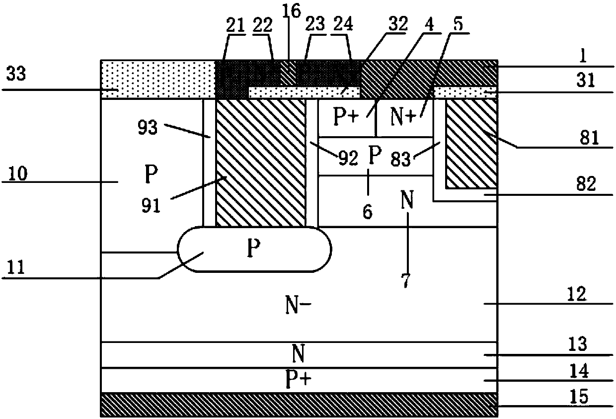
[0071] This example proposes a image 3 In the shown trench gate charge storage type insulated gate bipolar transistor, in this embodiment, in addition to setting a split electrode 84 under the gate electrode 81, which is isolated from it by a gate dielectric layer and has the same potential as the emitter metal 1, and the Except for the split electrode dielectric layer 85 which separates the split electrode 84 from the N-type charge storage layer 7 and the N-type drift region 12 , the other structures are the same as those in Embodiment 1.

[0072] In this embodiment, the shape of the split electrode is not limited. Specifically, the width of the split electrode 84 can be less than or equal to the width of the gate electrode 81; when the width of the split electrode 84 is smaller than the width of the gate electrode 81, it can A step-shaped split electrode dielectric layer is formed at the bottom of the trench, which further reduces the electric field concentration at the bot...

Embodiment 3

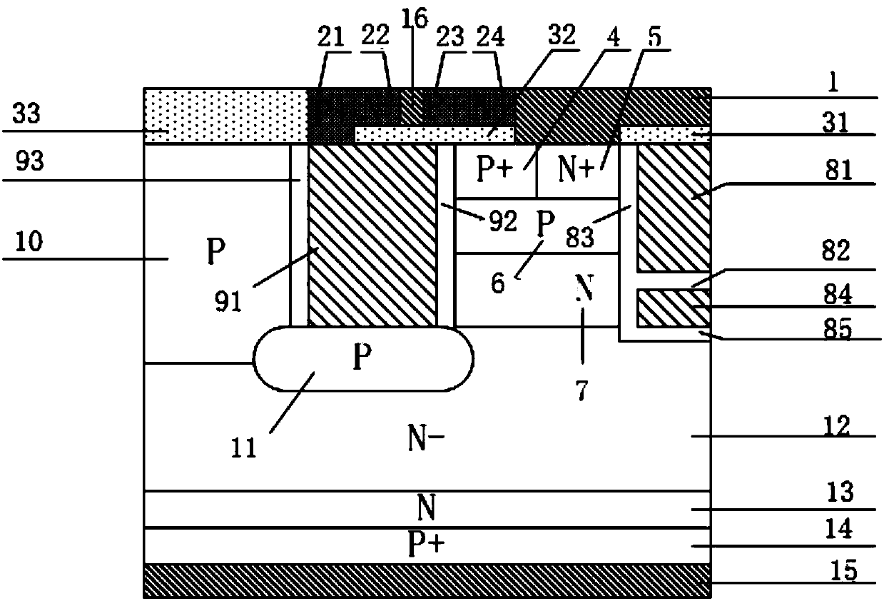
[0075] This example proposes a Figure 4 In the shown trench gate charge storage IGBT, the structure of this embodiment is the same as that of Embodiment 1 except that the second P-type layer 1102 is introduced at the bottom of the trench gate structure.

[0076] This embodiment can effectively shield the influence of negative charges in the N-type charge storage layer 7. On the one hand, it is beneficial to reduce the gate capacitance, on the other hand, it improves the concentration of the electric field at the bottom of the trench gate, and improves the breakdown voltage and reliability of the device.


PUM

PropertyMeasurementUnit
Thicknessaaaaaaaaaa
Thicknessaaaaaaaaaa

Abstract

The invention discloses a charge storage-type insulated gate bipolar transistor with a trench gate and a manufacturing method of the charge storage-type insulated gate bipolar transistor and belongs to the field of semiconductor power devices. A trench emitter structure is introduced into an N-type drift region of a traditional CSTBT structure, a P-type layer and a series diode structure are sequentially introduced to the lower part and the surface of the trench emitter structure, and meanwhile, the insulated gate bipolar transistor has a trench gate structure which partially penetrates into an N-type charge storage layer along the vertical direction, so that the problem of a contradictory relationship between the positive conduction performance and the voltage resistance of a device due to improvement of the doping concentration of the N-type charge storage layer in the traditional CSTBT is solved through the improvement; the saturation current density of the device is reduced and a short-circuit safety operation area of the device is improved; the switching speed of the device is improved and the switching loss is reduced; the breakdown voltage of the device is improved and the reliability is improved; compromise between a positive conduction voltage drop and the turn-off loss is optimized; and meanwhile, the manufacturing method of the device is compatible with a manufacturing technology of an existing CSTBT device.

Description

technical field [0001] The invention belongs to the technical field of semiconductor power devices, in particular to an insulated gate bipolar transistor (IGBT), in particular to a trench gate charge storage type insulated gate bipolar transistor (CSTBT). Background technique [0002] Insulated gate bipolar transistor (IGBT), as one of the core electronic components in modern power electronic circuits, is widely used in various fields such as transportation, communication, household appliances, and aerospace. Insulated gate bipolar transistor (IGBT) is a new type of power electronic device composed of an insulated field effect transistor (MOSFET) and a bipolar junction transistor (BJT), which can be equivalent to a MOSFET driven by a bipolar junction transistor. . IGBT combines the working mechanism of MOSFET structure and bipolar junction transistor. It not only has the advantages of MOSFET easy to drive, low input impedance, and fast switching speed, but also has the adva...

Claims


Application Information

Patent Timeline
IPC IPC(8): H01L29/10H01L29/739H01L21/336
Inventor 张金平赵倩刘竞秀李泽宏任敏张波
Owner UNIV OF ELECTRONIC SCI & TECH OF CHINA
Why Eureka
Try Eureka