Preparation method of enhanced field effect transistor based on two-dimensional planar heterojunction

A field-effect transistor, two-dimensional planar technology, applied in transistors, semiconductor/solid-state device manufacturing, electrical components, etc., can solve the problem of not being able to control device turn-off well, the carrier mobility has a great influence, and low switching. ratio and other issues, to achieve the effects of low power consumption, easy mass production, and low dark current

Inactive Publication Date: 2018-03-20
BEIJING UNIV OF TECH
View PDF3 Cites 8 Cited by
  • Summary
  • Abstract
  • Description
  • Claims
  • Application Information

AI Technical Summary

Problems solved by technology

Although single-layer graphene has unique electrical properties and excellent stability, it has excellent application potential in the field of microelectronics in the future, but graphene materials have a linear dispersion relationship near the Fermi level, and Klein tunneling occurs. Wear, resulting in devices made of materials with very low switching ratio
Although graphene can have a certain band gap by doping, etc., the carrier mobility is greatly affected by impurity scattering or defect effects; at the same time, it cannot be well controlled when used as a logic device channel material When the device is turned off, there will be leakage, etc.

Method used


Image

  • Preparation method of enhanced field effect transistor based on two-dimensional planar heterojunction
  • Preparation method of enhanced field effect transistor based on two-dimensional planar heterojunction
  • Preparation method of enhanced field effect transistor based on two-dimensional planar heterojunction

Examples


Embodiment 1

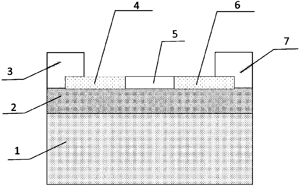
[0028] Embodiment 1 A preparation method based on a two-dimensional planar heterojunction enhanced field effect transistor is carried out according to the following steps:

[0029] The graphene grown on copper foil prepared by CVD method was transferred to the single crystal silicon wafer substrate with oxide layer by wet transfer method. During the experiment, ammonium persulfate solution was used as the etching solution for copper foil, and the concentration of the solution was 0.1mol / L. After the etching was completed, the graphene film was transferred to a new silicon dioxide / silicon substrate;

[0030] Spin photoresist evenly on the transferred graphene film, and then transfer the pattern on the mask plate to the photoresist by exposure through photolithography; then clean the unexposed part of the photoresist by developing solution Rinse off and tumble dry.

[0031] The non-patterned part is etched by plasma, and the part outside the pattern is etched away. After the e...


PUM

PropertyMeasurementUnit
thicknessaaaaaaaaaa
thicknessaaaaaaaaaa
thicknessaaaaaaaaaa

Abstract

The invention relates to a preparation method of an enhanced field effect transistor based on a two-dimensional planar heterojunction, and relates to the application field of microelectronic devices.The preparation method comprises the steps of transferring a graphene film to a monocrystalline silicon wafer substrate with an oxide layer by adopting wet transfer; uniformly spinning a photoresist on the graphene film, and transferring a pattern to the photoresist through exposure; etching the graphene film into graphene strips, and removing the photoresist; enabling the substrate with the graphene strips to serve as a substrate for growth, growing an MX2 type single-layer or few-layer material according to a CVD method, and forming a graphene-MX2-graphene in-plane heterojunction; and evaporating and depositing Ti/Au metal on the graphene-MX2-graphene in-plane heterojunction to obtain a two-dimensional planar heterojunction enhanced field effect transistor. The field effect transistor with a high switching ratio is obtained by combining the semi-metal material graphene with high carrier mobility and the MX2 two-dimensional material with the band gap being adjustable along with variations in number of layers, and the field effect transistor has excellent characteristics of very small dark current when being applied to photoelectric detection.

Description

technical field [0001] The invention relates to the application field of microelectronic devices, in particular to a method for preparing an enhanced field effect transistor with high switching ratio and low power consumption that can be used in digital logic circuits. technical background [0002] The successful preparation of graphene in 2004 proved that two-dimensional materials can exist stably in nature, and also started the research boom of two-dimensional nanomaterials. For two-dimensional materials, single-layer graphene has the thickness of a single atomic layer, and electrons are confined within the two-dimensional scale, making its electronic properties enhanced. Therefore, single-layer graphene has a high carrier mobility at room temperature, reaching 2.5×10 5 cn 2 V -1 the s -1 . Although single-layer graphene has unique electrical properties and excellent stability, it has excellent application potential in the field of microelectronics in the future, but ...

Claims


Application Information

Patent Timeline
Patent Type & Authority Applications(China)
IPC IPC(8): H01L21/336H01L21/34H01L29/06H01L29/16H01L29/24
CPCH01L29/0684H01L29/1606H01L29/24H01L29/66045H01L29/66969
Inventor 张永哲陈永锋严辉刘北云邓文杰游聪娅李景峰杨炎翰申高亮王光耀庞玮安博星
Owner BEIJING UNIV OF TECH
Why Eureka
Try Eureka