

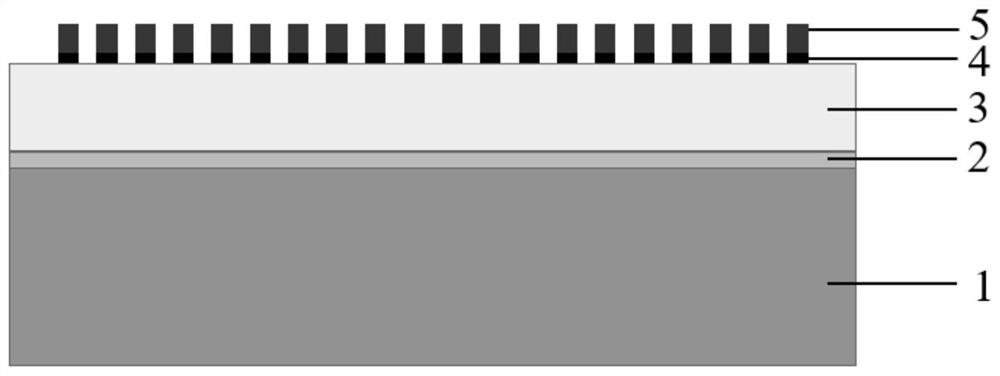
A surface acoustic wave device based on silicon carbide substrate/zinc oxide or doped zinc oxide thin film and its preparation method
A surface acoustic wave device and silicon carbide substrate technology, applied in the direction of electrical components, impedance networks, etc., can solve the problems of large propagation loss and consistency, deterioration of piezoelectric film quality, deterioration of device performance, etc., to achieve small temperature coefficient, The effect of high power tolerance and simple process steps
- Summary
- Abstract
- Description
- Claims
- Application Information
AI Technical Summary
Problems solved by technology
Method used
Image

Examples
Embodiment 1、6
[0044] Example 1. Preparation of surface acoustic wave devices by depositing zinc oxide on 6H-SiC single crystal substrate
[0045] 1) Clean the 6H-SiC single crystal substrate (thickness 500μm) with acetone, alcohol and deionized water for 4-8 minutes, and then immerse the substrate in HF:H 2 O (1:10, v / v) solution for 15 minutes to remove oxides on the surface of the substrate, then rinse with deionized water for 2 minutes, and finally blow dry with nitrogen, put it in a metal organic compound coating machine, and vacuumize to 1×10 -3 Pa; with TMGa (trimethylgallium), TMA1 (trimethylaluminum) and NH 3 (Ammonia gas) was used as gallium source, aluminum source and ammonia source respectively, and the V / III ratio was 1100. Under the conditions of 1100°C and growth pressure of 500Torr., Al with a thickness of 5nm was grown X Ga 1-X N intermediate transition layer. After the coating is finished, the temperature is lowered, and high-purity nitrogen is filled to atmospheric pres...
Embodiment 2
[0052] Example 2, Preparation of surface acoustic wave devices by depositing doped zinc oxide on 6H-SiC single crystal substrate
[0053] 1) Clean the 6H-SiC single crystal substrate (thickness 500μm) with acetone, alcohol and deionized water for 4-8 minutes, and then immerse the substrate in HF:H 2 O (1:10, v / v) solution for 15 minutes to remove oxides on the surface of the substrate, then rinse with deionized water for 2 minutes, and finally blow dry with nitrogen, put it in a metal organic compound coating machine, and vacuumize to 1×10 -3 Pa; with TMGa (trimethylgallium) and NH 3 (ammonia) as gallium and ammonia sources for the GaN epitaxial layer, respectively. The V / III ratio was 1100. Under the conditions of 1100° C. and a growth pressure of 500 Torr., a GaN intermediate transition layer with a thickness of 10 nm is grown. After the coating is finished, the temperature is lowered, and high-purity nitrogen is filled to atmospheric pressure. Open the cavity and take ...
PUM
| Property | Measurement | Unit |
|---|---|---|
| thickness | aaaaa | aaaaa |
| thickness | aaaaa | aaaaa |
| thickness | aaaaa | aaaaa |
Abstract
Description
Claims
Application Information