High-frequency high-performance acoustic surface wave device and preparation method thereof

A surface acoustic wave device and substrate technology, applied in the manufacture/assembly of piezoelectric/electrostrictive devices, device material selection, piezoelectric/electrostrictive/magnetostrictive devices, etc., can solve the problem of deteriorating device performance, Poor device uniformity, large propagation loss and other problems, to achieve the effect of huge application prospects, good consistency, and small propagation loss

Inactive Publication Date: 2018-09-04
TSINGHUA UNIV +1
View PDF6 Cites 17 Cited by
  • Summary
  • Abstract
  • Description
  • Claims
  • Application Information

AI Technical Summary

Problems solved by technology

Although the substrate or piezoelectric film has high sound velocity and thermal conductivity, it is expected to produce high-frequency and high-power devices, but the major defects of these substrates or piezoelectric films compared with single crystal substrates lead to large propagation loss and poor consistency
These reflect on the device that the Q value is small, the propagation loss is large, and the uniformity of the device is poor.
The reason is that these diamonds are polycrystalline materials, and the high density of crystal defects causes high propagation loss
In addition, the quality of the piezoelectric thin films grown on these substrates is far inferior to that of single crystal substrates, and crystal defects in the thin films further deteriorate the performance of the devices.

Method used


Image

  • High-frequency high-performance acoustic surface wave device and preparation method thereof
  • High-frequency high-performance acoustic surface wave device and preparation method thereof
  • High-frequency high-performance acoustic surface wave device and preparation method thereof

Examples


Embodiment 1

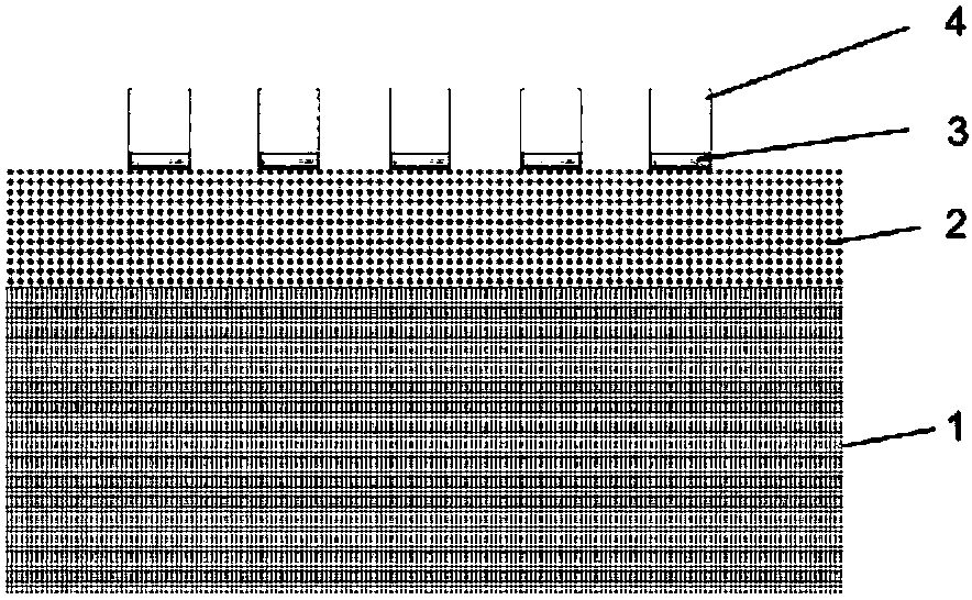
[0046] Example 1, YZ LiNbO 3 Fabrication of Surface Acoustic Wave Devices on Single Crystal Thin Film / 6H-SiC Single Crystal Substrate Structure

[0047] (1) 6H-SiC single crystal substrate (thickness 300μm), YZ LiNbO 3 The substrate was ultrasonically cleaned with acetone, alcohol, and deionized water for 5 minutes each, then rinsed with deionized water for 2 minutes, and finally dried with nitrogen gas.

[0048] (2) By direct bonding, the YZ LiNbO 3 The process surface of the substrate is contact-bonded with the smooth surface of the 6H-SiC single crystal substrate. The conditions of the direct bonding method are as follows: in a vacuum of 8.0×10 -5 Pa, the pressure is 800N, and annealing is carried out at 200°C for 5 hours to enhance the bonding force.

[0049] (3) Using the wafer grinding process, the YZ LiNbO 3thinned to 30 μm, and then chemically mechanically polished to 0.8 μm to obtain YZ LiNbO on 6H-SiC single crystal substrate 3 single crystal film.

[0050] (4...

Embodiment 2、42

[0058] Example 2, 42°Y-X LiTaO 3 Fabrication of Surface Acoustic Wave Devices on Single Crystal Thin Film / 6H-SiC Single Crystal Substrate Structure

[0059] (1) 6H-SiC single crystal substrate (thickness 500μm), 42°Y-X LiTaO 3 The substrate was ultrasonically cleaned with acetone, alcohol, and deionized water for 5 minutes each, then rinsed with deionized water for 2 minutes, and finally dried with nitrogen gas.

[0060] (2) Using the direct bonding method, the 42°Y-X LiTaO 3 The process surface of the substrate is contact-bonded with the smooth surface of the 6H-SiC single crystal substrate. The conditions of the direct bonding method are as follows: in a vacuum of 9.0×10 -5 Pa, the pressure is 800N, and annealing is carried out at 250°C for 8 hours to enhance the bonding force.

[0061] (3) Using the wafer grinding process, the 42°Y-X LiTaO 3 thinned to 50 μm, and then chemically mechanically polished to 0.2 μm to obtain 42°Y-X LiTaO on 6H-SiC single crystal substrate ...


PUM

PropertyMeasurementUnit
thicknessaaaaaaaaaa
thicknessaaaaaaaaaa
thicknessaaaaaaaaaa

Abstract

The invention discloses a high-frequency high-performance acoustic surface wave device and a preparation method thereof. The acoustic surface wave device comprises a silicon carbide monocrystal substrate, a piezoelectric thin film and an interdigital electrode which are stacked in sequence; the piezoelectric thin film is a lithium tantalate monocrystal thin film or a lithium niobate monocrystal thin film; and the silicon carbide monocrystal substrate is a 4H-SiC monocrystal substrate, a 6H-SiC monocrystal substrate, a 3C-SiC monocrystal substrate or a 3C-SiC epitaxial monocrystal substrate. The silicon carbide monocrystal substrate has relatively high sound velocity, excellent thermal stability and chemical stability and high heat conductivity; the lithium tantalate or lithium niobate piezoelectric monocrystal thin film is high in crystal quality, high in consistency and low in propagation loss; by adoption of the acoustic surface wave device with the interdigital electrode / lithium tantalate or lithium niobate monocrystal thin film / silicon carbide monocrystal substrate structural form, relatively high central frequency, high power tolerance and low temperature coefficient are achieved, so that the acoustic surface wave device has huge application prospect in the field of mobile communication.

Description

technical field [0001] The invention relates to a high-frequency high-performance surface acoustic wave device and a preparation method thereof, belonging to the technical field of information electronic materials. Background technique [0002] Surface acoustic wave (SAW) device is an important solid-state electronic device, which has the advantages of small size, light weight, and excellent signal processing capability. It is widely used in mobile communications, television broadcasting, and various military radar and communication systems. At the same time, great advances in semiconductor planar technology, material science, and microelectronics technology have enabled other types of SAW devices, such as various sensors, actuators, and microfluidic devices, to be used in remote control telemetry, aerospace, medical testing, and smart homes. It has also been widely used. From 2G, 3G, 4G to 5G era, the application frequency of mobile communication systems is getting higher ...

Claims


Application Information

Patent Timeline
Patent Type & Authority Applications(China)
IPC IPC(8): H01L41/047H01L41/18H01L41/22
CPCH10N30/87H10N30/85H10N30/01
Inventor 潘峰傅肃磊曾飞王为标李起宋成沈君尧
Owner TSINGHUA UNIV
Why Eureka
Try Eureka