Nanometer layered horizontal homogeneous PN diode and fabrication method and application thereof

A nano-layered, diode-based technology, applied in the direction of nanotechnology, final product manufacturing, sustainable manufacturing/processing, etc., can solve the problems of slow photoresponse, low success rate of homogeneous PN diodes, complex preparation process, etc., and achieve the preparation method Simple, no directional transfer process, good photoresponse effect

Inactive Publication Date: 2018-10-16
HUAZHONG UNIV OF SCI & TECH
View PDF7 Cites 13 Cited by
  • Summary
  • Abstract
  • Description
  • Claims
  • Application Information

AI Technical Summary

Problems solved by technology

[0005] The invention solves the technical problems of low success rate, complicated preparation process and slow photoresponse in preparing transition metal chalcogenide homogeneous PN diodes in the prior art

Method used


Image

  • Nanometer layered horizontal homogeneous PN diode and fabrication method and application thereof
  • Nanometer layered horizontal homogeneous PN diode and fabrication method and application thereof
  • Nanometer layered horizontal homogeneous PN diode and fabrication method and application thereof

Examples


preparation example Construction

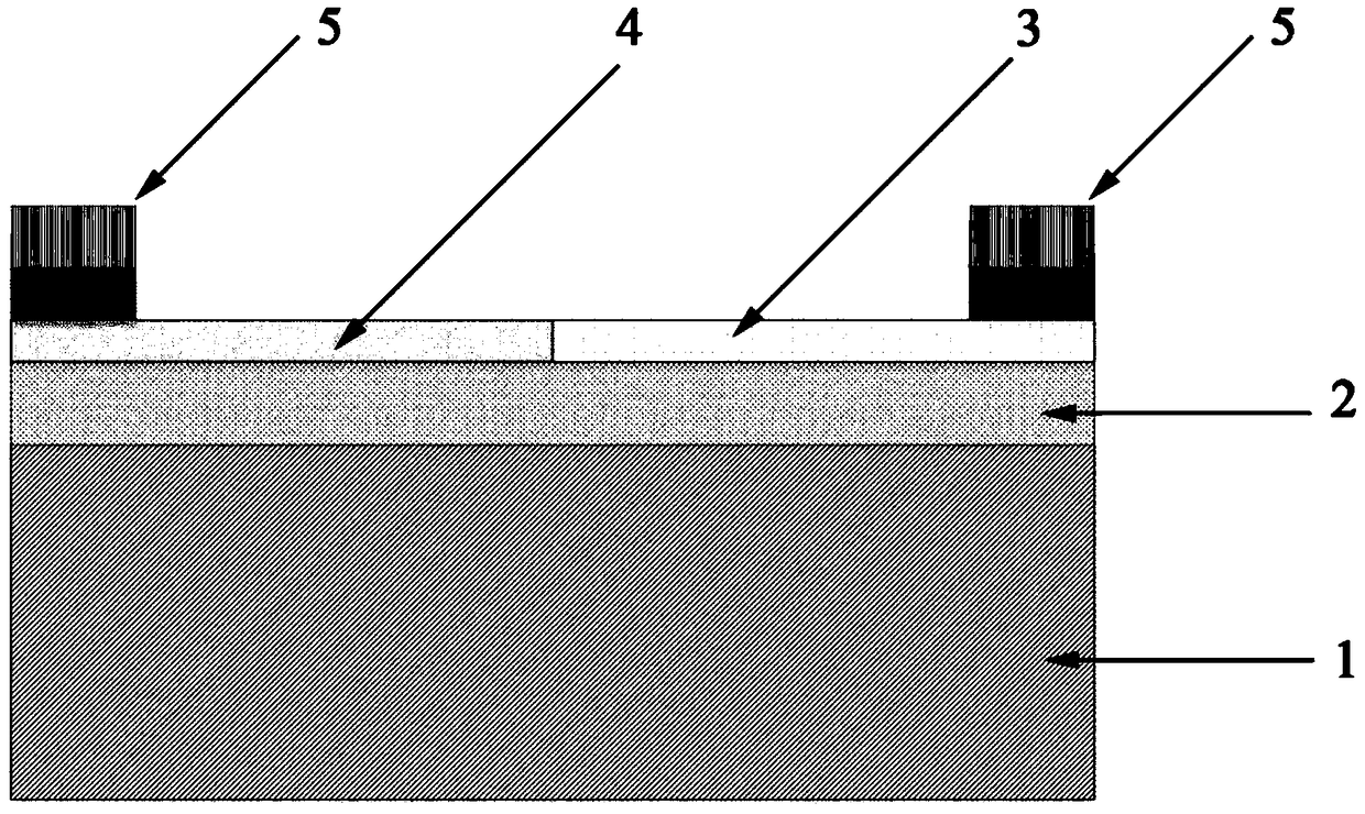
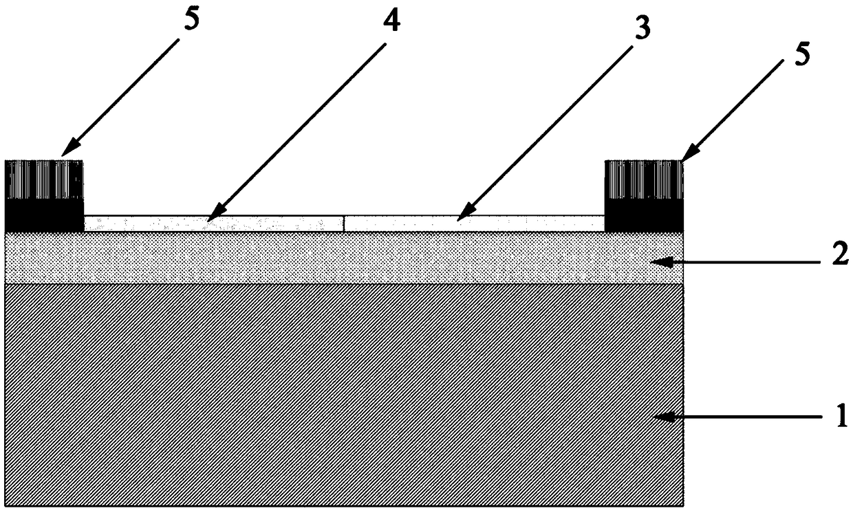
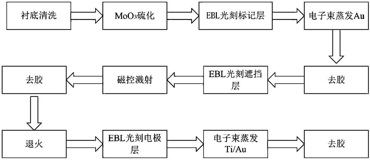
[0037] image 3 It is a flow chart of the process for preparing a horizontally homogeneous PN diode of a nano-layered transition metal chalcogenide compound in the present invention. Figure 4 It is the corresponding schematic diagram of the process flow chart of preparing nano-layered transition metal chalcogenide laterally homogeneous PN diodes in the present invention. The specific steps of the preparation method of the nano-layered transition metal chalcogenide laterally homogeneous PN diode provided by the present invention are as follows:

[0038] (1) Use acetone solution to have SiO on the surface 2 The p-type single crystal silicon wafer of the dielectric layer is ultrasonically cleaned to remove organic dirt on the substrate surface, and the substrate is ultrasonically cleaned with alcohol to remove acetone on the substrate surface, and rinsed with deionized water for 3 times.

[0039] (2) The above substrate is cleaned with buffered etchant BOE to remove the natura...

Embodiment 1

[0053] The invention discloses a method for preparing a nano-layered transition metal chalcogenide laterally homogeneous PN diode, comprising the following steps:

[0054] (1) Use acetone solution to have 50nm thick SiO on the surface 2 The thickness of the dielectric layer is 300 μm p-type single crystal silicon wafer, ultrasonic cleaning is performed to remove organic dirt on the substrate surface, and the substrate is ultrasonically cleaned with alcohol to remove acetone on the substrate surface, and deionized water is rinsed 3 times .

[0055] (2) The above substrate is cleaned with buffered etchant BOE to remove the natural oxide layer on the surface, then rinsed with deionized water, and dried with nitrogen. The cleaned surface has SiO 2 The single crystal silicon wafer of the dielectric layer is referred to as substrate A.

[0056] (3) For molybdenum trioxide powder MoO 3 n-type layered MoS was prepared on substrate A by chemical vapor deposition CVD with sulfur pow...

Embodiment 2

[0068] The invention discloses a method for preparing a nano-layered transition metal chalcogenide laterally homogeneous PN diode, comprising the following steps:

[0069] (1) Use acetone solution to have 80nm thick SiO on the surface 2 A p-type single crystal silicon wafer with a dielectric layer thickness of 325 μm was ultrasonically cleaned to remove organic dirt on the substrate surface, and the substrate was ultrasonically cleaned with alcohol to remove acetone on the substrate surface, and rinsed with deionized water for 3 Second-rate.

[0070] (2) The above substrate is cleaned with buffered etchant BOE to remove the natural oxide layer on the surface, then rinsed with deionized water, and dried with nitrogen. The cleaned surface has SiO 2 The single crystal silicon wafer of the dielectric layer is referred to as substrate A.

[0071] (3) For molybdenum trioxide powder MoO 3 n-type layered MoS was prepared on substrate A by chemical vapor deposition CVD with sulfur ...


PUM

PropertyMeasurementUnit
thicknessaaaaaaaaaa
thicknessaaaaaaaaaa
thicknessaaaaaaaaaa

Abstract

The invention discloses a nanometer layered horizontal homogeneous PN diode and fabrication method and application thereof. A p-type transition metal chalcogenide film and an n-type transition metal chalcogenide film both are arranged on an upper surface of a dielectric layer and are transversely connected, an electrode layer is longitudinally connected or transversely connected with the p-type transition metal chalcogenide film and the n-type transition metal chalcogenide film, and the p-type transition metal chalcogenide film and the n-type transition metal chalcogenide film comprises the same transition metal chalcogenide. The fabrication method is simple, high-efficiency and low-damage p-type doping of the transition metal chalcogenide is achieved through oxygen plasma by magnetron sputtering, effective and controllable doping is achieved, and the obtained diode is used for a photoelectric detector and has more rapid optical response and higher detection rate.

Description

technical field [0001] The invention belongs to the field of photodetectors, and more specifically relates to a nano-layered transition metal chalcogenide laterally homogeneous PN diode and its preparation method and application. Background technique [0002] Two-dimensional transition metal dichalcogenide layered materials (TMDs) have attracted much attention due to their extremely high electron mobility and other excellent optical, electrical, mechanical, chemical, acoustic, and mechanical properties. The chemical structures of transition metal chalcogenides are similar, and the properties of transition metal chalcogenides exhibiting semiconductor characteristics are also similar, for example, they all have band gaps that vary with the number of layers. in MoS 2 For example, MoS 2 It is an intrinsically n-type semiconductor material and the band gap (1.29eV-1.8eV) varies with the number of layers. MoS 2 It has excellent carrier mobility, and the single-layer carrier mo...

Claims


Application Information

Patent Timeline
Patent Type & Authority Applications(China)
IPC IPC(8): H01L31/0224H01L31/032H01L31/0352H01L31/103H01L31/18B82Y40/00
CPCB82Y40/00H01L31/022408H01L31/032H01L31/035281H01L31/103H01L31/18Y02P70/50
Inventor 曾祥斌王文照郭振宇吴少雄曾洋胡一说周广通靳雯任婷婷
Owner HUAZHONG UNIV OF SCI & TECH
Why Eureka
Try Eureka