A kind of self-driven photodetector and its preparation method
A photodetector and self-driven technology, applied in photovoltaic power generation, electric solid-state devices, semiconductor/solid-state device manufacturing, etc., can solve the problems of accelerating human skin aging, and achieve the effects of avoiding additional costs, improving light absorption, and fast response
- Summary
- Abstract
- Description
- Claims
- Application Information
AI Technical Summary
Problems solved by technology
Method used
Image
Examples
Embodiment 1
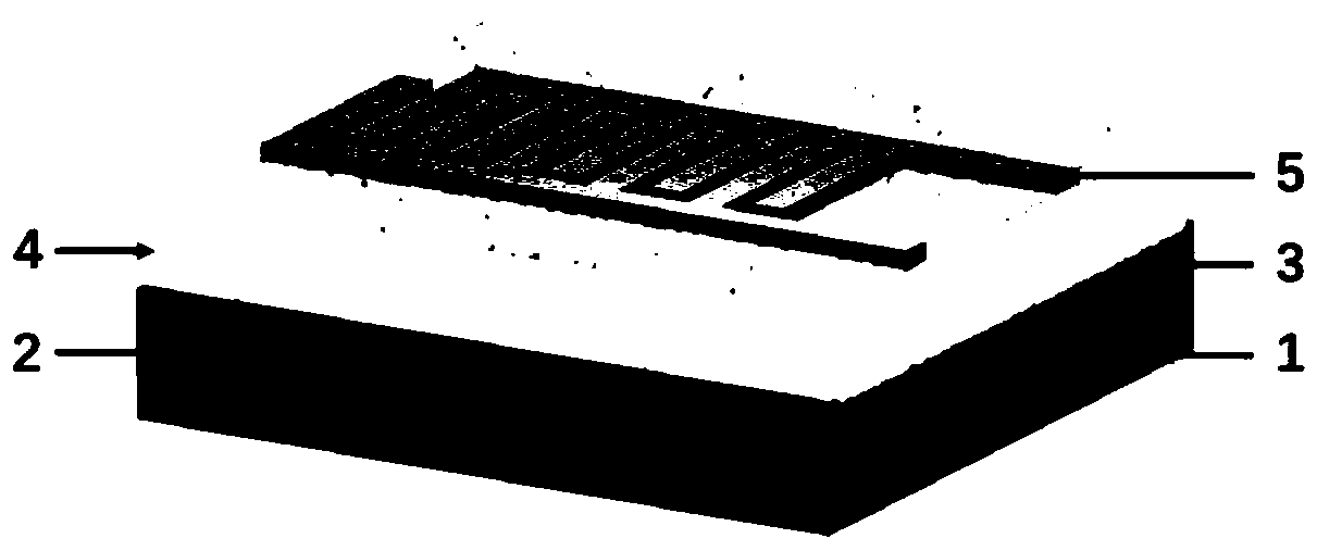
[0039]Cleaning of the substrate, in the present invention, the substrate can be a semiconductor substrate such as glass, PET, high-purity silicon, etc., and a PET substrate is mainly used in this embodiment. The substrate was cut into a suitable size (1cm×5cm), then ultrasonically cleaned with absolute ethanol and deionized water in an ultrasonic cleaner for 5 min, and then dried with nitrogen to obtain a clean substrate, and then at 100 ℃, heating for 10min.
[0040] The conductive layer can be gold, silver or ITO. The preparation of the conductive layer mainly uses ion sputtering technology or magnetron sputtering technology:
[0041] Ion sputtering technology: transfer the cleaned substrate into a vacuum chamber, and place a gold or silver target, the purity of the target is >99.999%, the vacuum degree of the reaction chamber during sputtering is better than 0.05mbar, the sputtering current is 20mA, and the sputtering current is 20mA. Shooting time 5min.
[0042] Magnetro...
Embodiment 2
[0056] Cleaning of the substrate, in the present invention, the substrate can be a semiconductor substrate such as glass, PET, high-purity silicon, etc., and a PET substrate is mainly used in this embodiment. The substrate was cut into a suitable size (1cm×5cm), then ultrasonically cleaned with absolute ethanol and deionized water in an ultrasonic cleaner for 5 min, and then dried with nitrogen to obtain a clean substrate, and then at 100 ℃, heating for 10min.
[0057] The conductive layer can be gold, silver or ITO. The preparation of the conductive layer mainly uses ion sputtering technology or magnetron sputtering technology:
[0058] Ion sputtering technology: transfer the cleaned substrate into a vacuum chamber, and place a gold or silver target, the purity of the target is >99.999%, the vacuum degree of the reaction chamber during sputtering is better than 0.05mbar, the sputtering current is 20mA, and the sputtering current is 20mA. Shooting time 5min.
[0059] Magnetr...
Embodiment 3
[0069] For the cleaning of the photodetector substrate, in the present invention, the substrate can be a semiconductor substrate such as glass, PET, high-purity silicon, etc., and glass is mainly used in this embodiment. Cut the substrate into a suitable size (1cm×5cm), then use acetone, anhydrous ethanol, and deionized water in an ultrasonic cleaner for ultrasonic cleaning for 5 minutes, and then dry it with nitrogen to obtain a clean substrate. At 100°C, heat for 10 min.
[0070] The conductive layer can be gold, silver or ITO. The preparation of the conductive layer mainly uses ion sputtering technology or magnetron sputtering technology:
[0071] Ion sputtering technology: transfer the cleaned substrate into a vacuum chamber, and place a gold or silver target, the purity of the target is >99.999%, the vacuum degree of the reaction chamber during sputtering is better than 0.05mbar, the sputtering current is 20mA, and the sputtering current is 20mA. Shooting time 5min.
[...
PUM
| Property | Measurement | Unit |
|---|---|---|
| thickness | aaaaa | aaaaa |
| thickness | aaaaa | aaaaa |
| thickness | aaaaa | aaaaa |
Abstract
Description
Claims
Application Information
 - R&D
- Intellectual Property
- Life Sciences
- Materials
- Tech Scout
- Unparalleled Data Quality
- Higher Quality Content
- 60% Fewer Hallucinations
Browse by: Latest US Patents, China's latest patents, Technical Efficacy Thesaurus, Application Domain, Technology Topic, Popular Technical Reports.
© 2025 PatSnap. All rights reserved.Legal|Privacy policy|Modern Slavery Act Transparency Statement|Sitemap|About US| Contact US: help@patsnap.com


