A preparation method of mems supercapacitor with controllable dielectric film thickness

A technology for supercapacitors and dielectric films, which is applied in the manufacture of hybrid/electric double layer capacitors, the manufacture of microstructure devices, and the process for producing decorative surface effects, etc. It can solve the problems of uniform deposition of dielectric films, complex processes, and high costs. problem, to achieve the effect of controllable dielectric film thickness, simple process and controllable thickness

Active Publication Date: 2020-09-15
TAIYUAN UNIV OF TECH
View PDF4 Cites 0 Cited by
  • Summary
  • Abstract
  • Description
  • Claims
  • Application Information

AI Technical Summary

Problems solved by technology

The traditional sol-gel method, magnetron sputtering method and other thin film preparation methods are limited by the substrate morphology, and it is difficult to achieve uniform deposition of dielectric thin films on three-dimensional grooved substrates. However, atomic layer deposition (ALD) does not Limited by the shape of the substrate, but this method has the disadvantages of complicated process, long time-consuming, high cost, etc.

Method used


Image

  • A preparation method of mems supercapacitor with controllable dielectric film thickness
  • A preparation method of mems supercapacitor with controllable dielectric film thickness
  • A preparation method of mems supercapacitor with controllable dielectric film thickness

Examples


Embodiment Construction

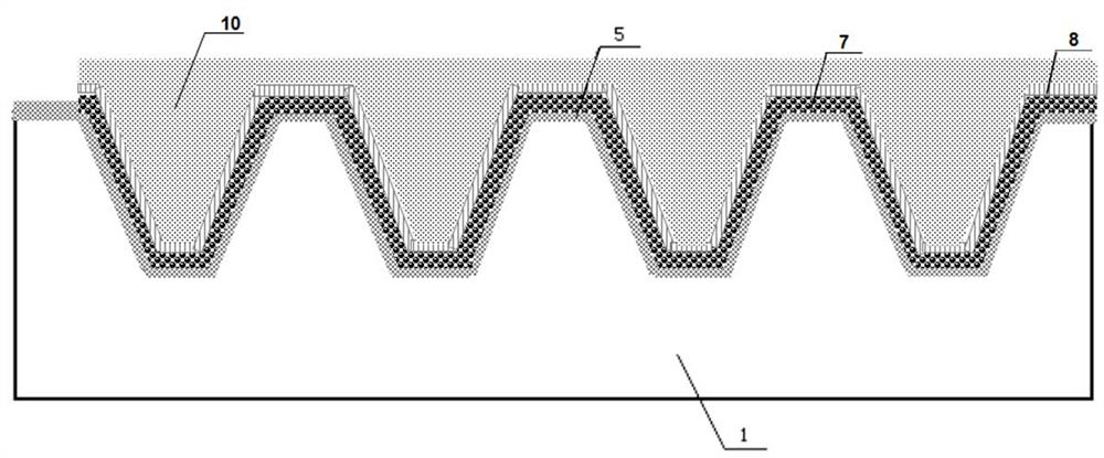
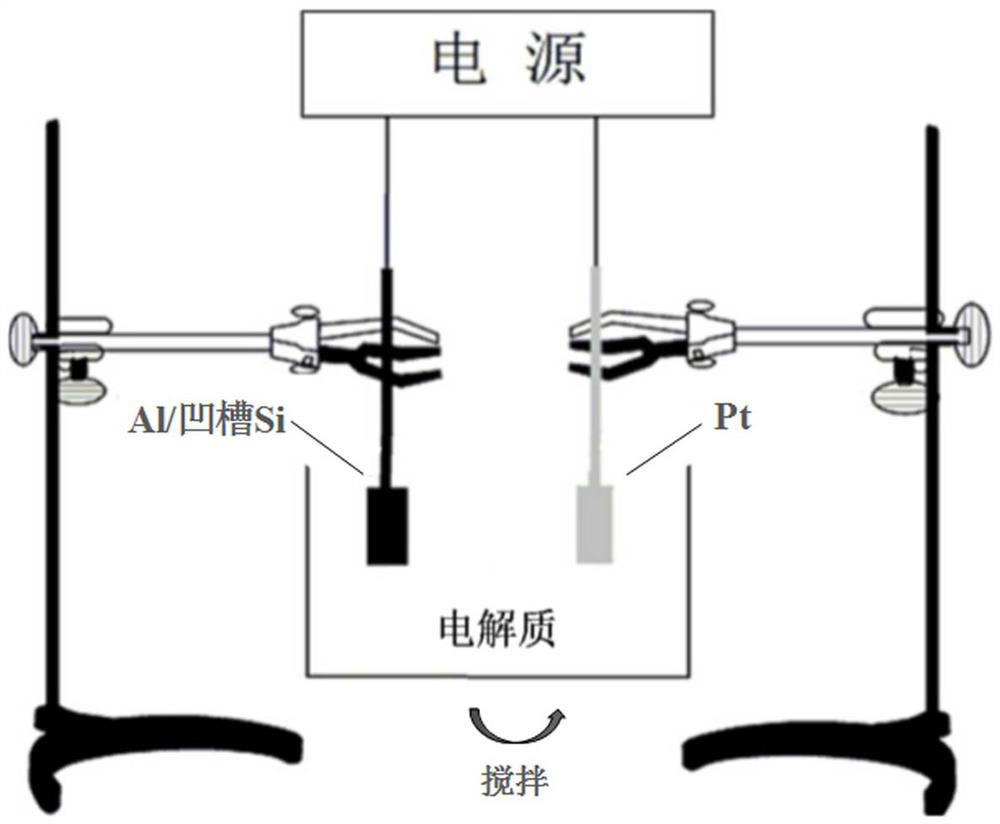
[0030] The MEMS electrostatic supercapacitor includes a silicon wafer 1, a three-dimensional groove array structure 4 is etched on the silicon wafer, an aluminum layer is sputtered on the etched silicon wafer as the lower electrode layer 5, and an anode is passed on the substrate of the sputtered aluminum layer. The oxidation method directly forms the aluminum oxide dielectric film layer 7, and then sputters the metal gold layer on the dielectric film layer 7 as the upper electrode layer 8, and the lower electrode layer 5 is partially exposed to the upper electrode layer 8, and the large specific surface area three-dimensional groove array structure 4 There is a filling layer 10 in the groove.

[0031] A method for preparing a MEMS supercapacitor with a controllable dielectric film thickness, comprising the steps of:

[0032] 1. Select a 4-inch silicon wafer 1 as the substrate, and wash the silicon wafer 1 in xylene, acetone, alcohol, sulfuric acid / hydrogen peroxide, ammonia / h...


PUM


Abstract

The invention belongs to the technical field of micro-energy manufacture and specifically relates to a preparation method of a MEMS supercapacitor with a controllable dielectric film. The method firstly adopts a wet etching process to etch a three-dimensional groove array structure on a silicon substrate to serve as a carrier of the electrode, thereby remarkably increasing the specific surface area of the electrode and improving the capacitive characteristic of the supercapacitor, and being easy to integrate and manufacture on the other hand; according to the anodic oxidation method, a thickness-controllable Al2O3 thin film can be directly formed on the basis of the electrode thin film and served as a dielectric layer of the capacitor; the method is simple in process, controllable in thickness and not limited by the morphology of the substrate. According to the wet etching technology of the silicon wafer, the depth-width ratio of the groove can be controlled; proper groove width and height are designed, thereby greatly increasing the specific surface area of the electrode. Compared with the traditional electrostatic capacitor, the electrostatic supercapacitor prepared on the basisof the anodic oxidation method and the groove array-etched substrate has great advantages in both process cost and performance aspects.

Description

technical field [0001] The invention belongs to the technical field of micro-energy manufacturing, and relates to a method for preparing a MEMS electrostatic supercapacitor with simple process, controllable dielectric film thickness and high energy density applied in a microsystem, specifically a MEMS with controllable dielectric film thickness Preparation method of supercapacitor. [0002] technical background [0003] Micro Electro Mechanical System (MEMS), referred to as MEMS, is a new type of interdisciplinary technology developed in recent years. It integrates functions such as microstructure, microsensor, microactuator, micropower supply and signal processing control. , has the advantages of low cost, small size, strong self-control, and high reliability. It is a cutting-edge technology in the 21st century based on micro / nano technology. Among them, the micro power supply is the key basic component in the MEMS, and the miniaturization and integration of the power suppl...

Claims


Application Information

Patent Timeline
Patent Type & Authority Patents(China)
IPC IPC(8): B81C1/00H01G11/84
CPCB81C1/0038H01G11/84Y02E60/13
Inventor 李刚段淑斐李廷鱼王开鹰赵清华李朋伟胡杰张文栋
Owner TAIYUAN UNIV OF TECH
Why Eureka
Try Eureka