Broadband active feedback transimpedance amplifier for low voltage operation

A technology of transimpedance amplifier and active feedback, applied in amplifiers with semiconductor devices/discharge tubes, DC-coupled DC amplifiers, amplifiers, etc., can solve problems such as insufficient voltage margin, and achieve extended bandwidth and large output voltage The effect of swing and cost reduction

Active Publication Date: 2018-12-11
TIANJIN UNIV
View PDF13 Cites 2 Cited by
  • Summary
  • Abstract
  • Description
  • Claims
  • Application Information

AI Technical Summary

Problems solved by technology

[0007] On the basis of analyzing the advantages and disadvantages of adjustable cascode (RGC) transimpedance amplifiers, the present invention proposes a low-voltage, high-bandwidth active feedback transimpedance amplifier for the front end of an optical receiver. The very active feedback connection method is used to overcome the problem of insufficient voltage margin in the advanced process of the regulated cascode (RGC) structure. See the following description for details:

Method used


Image

  • Broadband active feedback transimpedance amplifier for low voltage operation
  • Broadband active feedback transimpedance amplifier for low voltage operation
  • Broadband active feedback transimpedance amplifier for low voltage operation

Examples


Embodiment 1

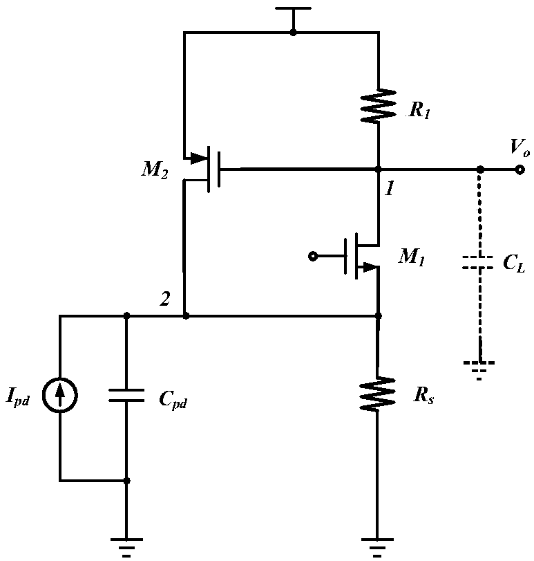
[0036] A broadband active feedback transimpedance amplifier for low-voltage operation, see figure 2 , the amplifier consists of:

[0037] 1. Use a fixed bias to replace the grid bias of the common grid input transistor of the adjustable cascode (RGC) structure to reduce the consumption of voltage margin.

[0038] That is, the consumption of a MOS transistor threshold voltage on the power supply voltage is reduced.

[0039] 2. Use a common-gate input terminal with common-source active feedback to achieve an input impedance similar to that of a regulated cascode (RGC) structure, thereby isolating the influence of input parasitic capacitance on bandwidth.

[0040] That is, in figure 2 The middle node 2 is the signal input terminal. Observing from this node to the inside of the circuit, it can be seen that the common gate input terminal with common source active feedback is used.

[0041] 3. Add a capacitive degeneration circuit to generate a zero point that cancels the pole ...

Embodiment 2

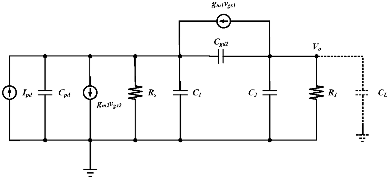
[0044] Attached below Figure 1-Figure 5 The scheme in Example 1 is further introduced, see the following description for details:

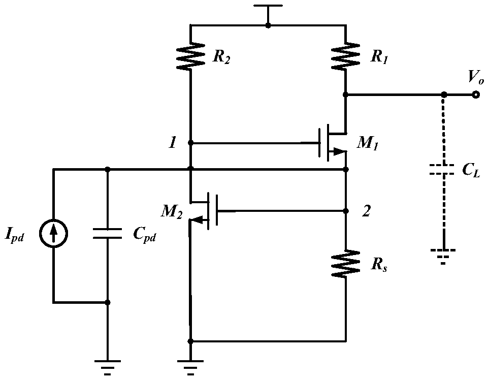
[0045] figure 1 Shown is the circuit schematic of a regulated cascode (RGC) transimpedance amplifier. The circuit consists of a resistor R 1 , resistance R s and MOS tube M 1 constitutes a common-gate main amplifier, with resistor R 2 and MOS tube M 2 The common-source auxiliary amplifier composed of two parts.

[0046] Among them, the main function of the entire transimpedance amplifier is to receive the weak current signal output by the photodetector, and convert and amplify it into a voltage signal. Before discussing the circuit designed in the embodiment of the present invention, some characteristics of the regulatory cascode (RGC) structure will be described first.

[0047] First analyze the DC operating point. To ensure the stable operation of the overall circuit, it is necessary to ensure that all MOS tubes work in the saturation reg...


PUM


Abstract

The invention discloses a wide-band active feedback transimpedance amplifier for low voltage operation. The amplifier is composed of a common-grid main amplifier composed of a resistor R1, a resistorRs and a MOS transistor M1, and a common-source active feedback circuit composed of a MOS transistor M2. A bias voltage is added to the gate of the MOS transistor M1 of the transimpedance amplifier, thereby replacing the gate bias of the common gate input transistor of the regulating cascode structure and reducing the voltage redundancy consumption; The transimpedance amplifier uses a common-gateinput terminal with common-source active feedback to achieve an input impedance similar to that of a regulated cascode structure, thereby isolating the effect of input parasitic capacitance on the bandwidth. A capacitive degradation circuitry is added to the transimpedance amplifier to produce zero points that cancel poles, extending bandwidth while increasing the gain of the voltage. The invention can realize the monolithic integration of the analog front end and the digital signal processing back end of the optical receiver with high performance on the same chip, reduce the cost and enhancethe function.

Description

technical field [0001] The invention belongs to optical communication, optical interconnection and visible light communication systems, and relates to a transimpedance amplifier adopting an active feedback design. Background technique [0002] With the continuous improvement of social informatization, broadband services represented by big data carriers such as the Internet of Things, cloud computing, and mobile Internet are booming, which has doubled the demand for network bandwidth and data traffic in human society. In order to meet the transmission of massive information, breakthroughs have been made in ultra-high-speed, ultra-large-capacity optical fiber communication technology for trunk network transmission. However, limited by technology and cost, the "last mile" of optical fiber communication has not been well resolved. [0003] In optical fiber communication systems, for optical receivers, monolithic integration of photodiodes and amplifier circuits on the same subs...

Claims


Application Information

Patent Timeline
Patent Type & Authority Applications(China)
IPC IPC(8): H03F1/30H03F3/45
CPCH03F1/301H03F3/45179
Inventor 谢生闵闯毛陆虹
Owner TIANJIN UNIV
Why Eureka
Try Eureka