Synthesis method and application of dialkynyl bridged monoperylene imide dimer n-type semiconductor material

A monoperylene imide dimer, n-type semiconductor technology, applied in semiconductor devices, semiconductor/solid-state device manufacturing, electric solid-state devices, etc., can solve the problems of cumbersome synthesis process, difficult purification, harsh reaction conditions, etc. Wide application prospects, high conversion efficiency, and the effect of large electron affinity

Inactive Publication Date: 2019-01-15
HENAN NORMAL UNIV
View PDF4 Cites 7 Cited by
  • Summary
  • Abstract
  • Description
  • Claims
  • Application Information

AI Technical Summary

Problems solved by technology

At present, the derivatives of perylene monoimide cannot be synthesized in large quantities in the laboratory and industry, the reaction conditions are extremely harsh, or the reaction steps are as high as 8-9 steps, the synthesis process is cumbersome and the purification is extremely difficult

Method used


Image

  • Synthesis method and application of dialkynyl bridged monoperylene imide dimer n-type semiconductor material
  • Synthesis method and application of dialkynyl bridged monoperylene imide dimer n-type semiconductor material
  • Synthesis method and application of dialkynyl bridged monoperylene imide dimer n-type semiconductor material

Examples


Embodiment 1

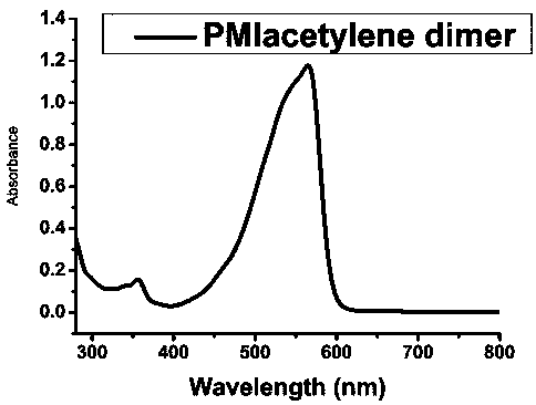
[0019] Under anaerobic conditions, use high-purity nitrogen to exhaust the air in the reaction vessel, add 3.2mmol of compound M1, 2.1mmol of cuprous iodide and 500mL of tetrahydrofuran into the reaction vessel, isolate the air and inject 50mL of anhydrous triethylamine, and then add 0.43 mmolPd (PPh 3 ) 4 Catalyst, after exhausting the oxygen, stir the mixture at 71°C for 72h, then lower it to 25°C and let it stand for 24h to turn into a red organic gel, then add 1L of deionized water and 500mL of dichloromethane in turn, shake fully and filter, filter The cake was washed 3 times with anhydrous methanol, and then the filter cake was vacuum-dried to obtain red needle-shaped crystals, which were dried in the air to obtain the small molecule semiconductor material perylene monoimide N-2-octyl-dodecyl-diacetylene Base-perylene monoimide N-2-octyl-dodecyl compound.

[0020] The ultraviolet-visible absorption spectrum figure of the small molecular semiconductor material prepared ...

Embodiment 2

[0022] Under anaerobic conditions, use high-purity nitrogen to exhaust the air in the reaction vessel, add 6.24mmol of compound M2, 4.2mmol of cuprous iodide and 700mL of tetrahydrofuran into the reaction vessel, isolate the air and inject 50mL of anhydrous triethylamine, and then add 0.61 mmolPd (PPh 3 ) 4 Catalyst, after exhausting the oxygen, stir the mixture at 71°C for 72h, then lower it to 25°C and let it stand for 24h to turn into a red organic gel, then add 1L of deionized water and 500mL of dichloromethane in turn, shake fully and filter, filter The cake was washed 3 times with anhydrous methanol, and the filter cake was vacuum-dried to obtain red needle-shaped crystals, which were dried in the air to obtain the small molecule semiconductor material perylene monoimide N-2-ethyl-hexyl-bisethynyl-perylene Monoimide N-2-ethyl-hexyl compound.

Embodiment 3

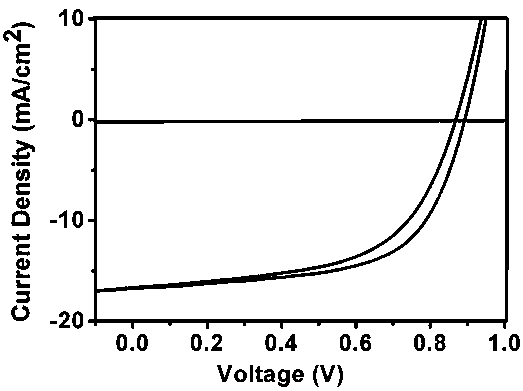
[0024] 1.5g of the small molecule semiconductor material perylene monoimide N-2-octyl-dodecyl-bisethynyl-perylene monoimide N-2-octyl-dodecyl obtained in Example 1 Mix the compound with 8.5g ITIC evenly, add 1L o-dichlorobenzene to dissolve, add 10g PBDB-T and heat to 110°C and stir for 2h, and prepare a layer thickness of 110nm thin film, and then vapor-deposit a molybdenum oxide hole transport layer with a thickness of 8nm and silver with a thickness of 100nm by vacuum evaporation to prepare a metal electrode on it, and finally obtain an organic solar cell.

[0025] In the simulated sunlight (the xenon light source purchased from Beijing Changtuo Technology Co., Ltd., without filters, and the irradiance meter purchased by Beijing Normal University Optical Instrument Factory for calibration, the light intensity is 100mW / cm 2 ), the short-circuit current of the organic solar cell is 18mA / cm 2 , the open circuit voltage is 0.88V, the fill factor is 0.60, and the energy convers...


PUM


Abstract

The invention discloses a synthesis method and application of a dialkynyl bridged monoperylene imide dimer n-type semiconductor material, and belongs to the technical fields of synthesis of organic semiconductor n-type materials and application of the organic semiconductor n-type materials in photoelectric functional devices. The main technical point comprises that the synthesis of the dialkynyl bridged monoperylene imide dimer n-type semiconductor material particularly includes synthesis of a perylene monoimide N-2-octyl-dodecyl-diacetyl-perylene monoimide N-2-octyl-dodecyl compound and synthesis of a perylene monoimide N-2-ethyl-hexyl-diacetyl-perylene monoimide N-2-ethyl-hexyl compound, and the invention particularly discloses the application of the dialkynyl bridged monoperylene imidedimer n-type semiconductor material in organic solar cells. The synthesis process is simple and feasible, and the yield is high. The synthesized dialkynyl bridged monoperylene imide dimer n-type semiconductor material has excellent performance and can obtain good application in photoelectric functional devices.

Description

technical field [0001] The invention belongs to the technical field of synthesis of organic semiconductor n-type materials and their application in photoelectric functional devices, and in particular relates to a synthesis method and application of bis-alkynyl bridged monoperyleneimide dimer n-type semiconductor materials. Background technique [0002] Organic semiconductor n-type materials are widely used in organic solar cells, field effect transistors, photodetectors, flexible plastic thin film electronic products, thin film displays, etc. These materials are usually composed of aromatic heterocyclic conjugated systems. Common small molecule n-type organic semiconductor materials include fullerene derivatives, phthalocyanines, perylene derivatives, and naphthalimides. Compared with polymers, small molecules with a defined structure are easy to synthesize and purify, have less residual catalyst pollution, are convenient to apply, and can have a variety of processing option...

Claims


Application Information

Patent Timeline
Patent Type & Authority Applications(China)
IPC IPC(8): C07D221/18H01L51/00H01L51/46
CPCC07D221/18H10K85/6572Y02E10/549
Inventor 秦瑞平郭得恩杨纪恩蒋玉荣
Owner HENAN NORMAL UNIV
Why Eureka
Try Eureka