Preparation method of supporting type film bulk acoustic wave resonator
A thin-film bulk acoustic wave and resonator technology, which is applied in the direction of electrical components and impedance networks, can solve problems such as large residual stress of single-crystal thin films, lower yield, and cracks caused by wafer warping, so as to eliminate loss phenomena and alleviate Lattice mismatch and thermal mismatch, effects of improving stress state and crystal quality
- Summary
- Abstract
- Description
- Claims
- Application Information
AI Technical Summary
Problems solved by technology
Method used
Image
Examples
Embodiment 1
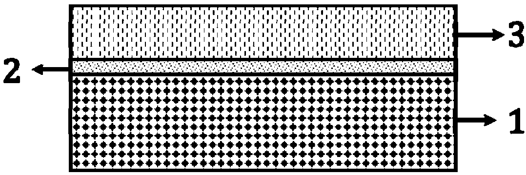
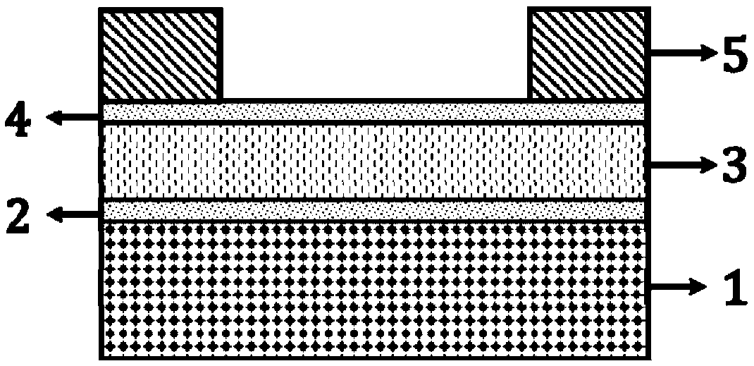
[0047] The preparation method of the supported film bulk acoustic resonator of this embodiment includes the following steps:
[0048] (1) On the (111) plane Si substrate, grow a Mo metal insertion layer by radio frequency magnetron sputtering or molecular beam epitaxy;
[0049] (1-1) Cleaning: choose (111) Si substrate 1 through concentrated H 2 SO 4 :H 2 o 2 :H 2 O(1:1:3) and BOE:HF(20:1) cleaning to remove surface organic matter;
[0050] (1-2) Annealing: put the (111) Si substrate under a pressure of 3.0×10 -10 In Torr’s high-vacuum growth chamber, bake at 750°C for 30-60 minutes to remove pollutants on the substrate surface;
[0051] (1-3) Using a radio frequency magnetron sputtering machine, metal Mo with a purity of 99.99% is used as a sputtering target, and high-purity Ar (99.999%) is introduced as a sputtering gas during sputtering, and the total working pressure is 3~10Pa, target base distance is set to 60mm, vacuum degree is 4.0×10 -4 Pa, the substrate temper...
Embodiment 2
[0064] A preparation method of a supported film bulk acoustic resonator, comprising the following steps:
[0065] (1) On the cleaned and annealed (111) Si substrate, the Mo metal insertion layer is grown by radio frequency magnetron sputtering or molecular beam epitaxy, specifically:
[0066] Using a radio frequency magnetron sputtering machine, metal Mo is used as the sputtering target, and Ar gas is introduced as the sputtering gas during sputtering. at 4.0×10 -4 Pa, the substrate temperature is 150° C.-250° C. and a Mo metal insertion layer with a thickness of 100-200 nm is grown.
[0067] The cleaning is specifically: through concentrated H 2 SO 4 :H 2 o 2 :H 2 O=1:1:3 mixed solution and BOE:HF=20:1 mixed solution are cleaned to remove surface organic matter.
[0068] The annealing is specifically:
[0069] Place the substrate at a pressure of 2.5×10 -10 -3.0×10 -10 In Torr's high-vacuum growth chamber, bake at a high temperature of 600-750°C for 30-60 minutes to...
Embodiment 3
[0085] A preparation method of a supported film bulk acoustic resonator, comprising the following steps:
[0086] (1) On the cleaned and annealed (111) Si substrate, the Mo metal insertion layer is grown by radio frequency magnetron sputtering or molecular beam epitaxy, specifically:
[0087] Using a radio frequency magnetron sputtering machine, metal Mo is used as the sputtering target, Ar gas is introduced as the sputtering gas during sputtering, the total working pressure is 10Pa, the target base distance is set to 70mm, and the vacuum degree is higher than 4.0×10 -4 Pa, and the substrate temperature is 250°C to grow a Mo metal insertion layer with a thickness of 200nm.
[0088] The cleaning is specifically: through concentrated H 2 SO 4 :H 2 o 2 :H 2 O=1:1:3 mixed solution and BOE:HF=20:1 mixed solution are cleaned to remove surface organic matter.
[0089] The annealing is specifically:
[0090] Place the substrate at a pressure of 2.5×10 -10In Torr's high-vacuum ...
PUM
| Property | Measurement | Unit |
|---|---|---|
| Thickness | aaaaa | aaaaa |
| Thickness | aaaaa | aaaaa |
| Thickness | aaaaa | aaaaa |
Abstract
Description
Claims
Application Information


