
All-solid-state organic electrochemical phototransistor and preparation method thereof

A phototransistor and all-solid-state technology, which is applied in semiconductor/solid-state device manufacturing, electrical solid-state devices, circuits, etc., can solve problems such as difficult integration of electronic devices, volatile liquid electrolytes, and unstable device performance, achieving significant economic and Social benefits, beneficial to popularization and application, excellent photoelectric performance

Inactive Publication Date: 2019-04-16
FUZHOU UNIV
View PDF3 Cites 4 Cited by
  • Summary
  • Abstract
  • Description
  • Claims
  • Application Information

AI Technical Summary

Problems solved by technology

However, at present, all electrochemical transistors use liquid electrolytes, the process is relatively complicated, and the volatile characteristics of liquid electrolytes not only cause unstable device performance, but also are difficult to integrate into existing solid-state electronic devices, which seriously affect the current state of the art. Applications of chemical transistors
At present, there is no report on the preparation of all-solid-state organic electrochemical phototransistors combined with high transconductance electrochemical transistors.

Method used


Image

  • All-solid-state organic electrochemical phototransistor and preparation method thereof
  • All-solid-state organic electrochemical phototransistor and preparation method thereof
  • All-solid-state organic electrochemical phototransistor and preparation method thereof

Examples


Embodiment 1

[0025] 1) Wash the cut 1.5cm×1.5cm heavily doped P-type silicon wafer with acetone, isopropanol, chloroform, and distilled water (three times), and dry it with nitrogen to obtain a clean silicon wafer Make the base.

[0026] 2) Preparation of ion gel electrolyte: polyacrylonitrile, lithium bistrifluoromethanesulfonimide, ethylene carbonate and propylene carbonate were mixed in a mass ratio of 14.1:3.9:41:41 and heated in a 90°C water bath. Stir until clear, transparent colloidal gel state;

[0027] 3) Use a syringe to cover the silicon wafer with the electrolyte gel prepared in step 2), and then use a low speed of 500rpm (5s) and a high speed of 3500rpm (45s) to spin the solution to form a uniform film on the silicon wafer, and then place the silicon wafer Move it into a vacuum drying oven at 120°C for annealing for 10 hours to form a 2 μm electrolyte layer.

[0028] 4) Spin-coat the dispersion of PEDOT:PSS at 1000rpm (60s) to prepare the active layer, and then anneal at 120...

Embodiment 2

[0032] 1) Wash the cut 1.5cm×1.5cm heavily doped P-type silicon wafer with acetone, isopropanol, chloroform, and distilled water (three times), and dry it with nitrogen to obtain a clean silicon wafer Make the base.

[0033] 2) Preparation of ion gel electrolyte: polyacrylonitrile, lithium bistrifluoromethanesulfonimide, ethylene carbonate and propylene carbonate were mixed in a mass ratio of 14.1:3.9:41:41 and heated in a 90°C water bath. Stir until clear, transparent colloidal gel state;

[0034] 3) Use a syringe to spread the electrolyte prepared in step 2) on the edge of the junction between the scraper and the silicon wafer. The distance between the scraper and the silicon substrate is 200 μm, and the scraping speed is 20 mm / s. After forming a uniform film, move it into a vacuum drying oven for annealing at 120 ° C for 10 h .

[0035] 4) On the basis of step 3), spread the PEDOT:PSS dispersion on the edge of the junction between the scraper and the silicon wafer. The di...


PUM


Abstract

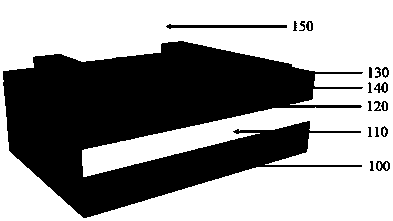
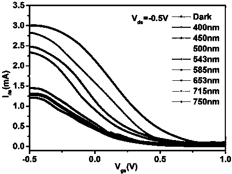
The invention relates to an all-solid-state organic electrochemical phototransistor and a preparation method thereof. The organic electrochemical phototransistor adopts a bottom gate planar structure,and the device includes a substrate, a solid electrolyte layer, an active layer, a source / drain electrode and a light absorbing layer from bottom to top; the solid electrolyte layer uses a polymer ion gel electrolyte and utilizes a spin coating or knife coating process to form a solid electrolyte layer on the substrate to achieve an all-solid-state organic electrochemical phototransistor. The all-solid-state organic electrochemical phototransistor provided by the invention achieves excellent optical response R and detection rate D under low voltage operation, and the characteristics of the all-solid-state phototransistor can be further integrated into advanced electronic and circuit systems, and the application field of the high performance electrochemical transistor is expanded. The all-solid-state organic electrochemical transistor is expected to be widely used in the fields of optical sensors, artificial synapses, and large-scale integrated circuits.

Description

technical field [0001] The invention belongs to the technical field of electronic materials and devices, and relates to an all-solid-state organic electrochemical phototransistor and a preparation method thereof. Background technique [0002] Organic field-effect phototransistors have received extensive attention, but the improvement of their photoelectric properties mainly focuses on the optimization of active layer materials, including: n / p-type semiconductor material blending, n / p-type semiconductor material layer heterojunction, etc. . In fact, the improvement of the performance of organic field-effect phototransistors is limited by the mobility of organic semiconductor materials, and more importantly, the nature of low transconductance of field-effect transistors. At the same time, the operating voltage of most organic field-effect phototransistors is higher than 10V, which generates large power consumption and is not conducive to integration into wearable devices, whi...

Claims


Application Information

Patent Timeline
Patent Type & Authority Applications(China)
IPC IPC(8): H01L51/42H01L51/46H01L51/48
CPCH10K71/12H10K71/40H10K85/1135H10K30/65Y02E10/549
Inventor 陈惠鹏严育杰郭太良巫晓敏陈奇珍刘亚倩
Owner FUZHOU UNIV
Learn More