A manufacturing method of a field emission ion neutralizer chip based on an SOI process

A manufacturing method and field emission technology, which are applied in the manufacture of discharge tubes/lamps, electrode system manufacture, and utilization of plasma, etc., can solve the problems of damage to the structure of the emitter, poor thermal conductivity, influence on stability and life, etc. The effect of reducing power consumption, improving emission efficiency, and preventing short circuit of cathode grid

Active Publication Date: 2019-05-31
HUAZHONG UNIV OF SCI & TECH
View PDF8 Cites 12 Cited by
  • Summary
  • Abstract
  • Description
  • Claims
  • Application Information

AI Technical Summary

Problems solved by technology

However, there are several key technical issues of the field emission neutralizer that are still unresolved: first, the field shielding effect - because of its inhomogeneity, only a part of the nanomaterial can effectively emit under a strong electric field, while due to the local current density If it is too large, it is easy to be dama

Method used


Image

  • A manufacturing method of a field emission ion neutralizer chip based on an SOI process
  • A manufacturing method of a field emission ion neutralizer chip based on an SOI process
  • A manufacturing method of a field emission ion neutralizer chip based on an SOI process

Examples


Embodiment Construction

[0034] In order to make the object, technical solution and advantages of the present invention clearer, the present invention will be further described in detail below in conjunction with the accompanying drawings and embodiments. It should be understood that the specific embodiments described here are only used to explain the present invention, not to limit the present invention. In addition, the technical features involved in the various embodiments of the present invention described below can be combined with each other as long as they do not constitute a conflict with each other.

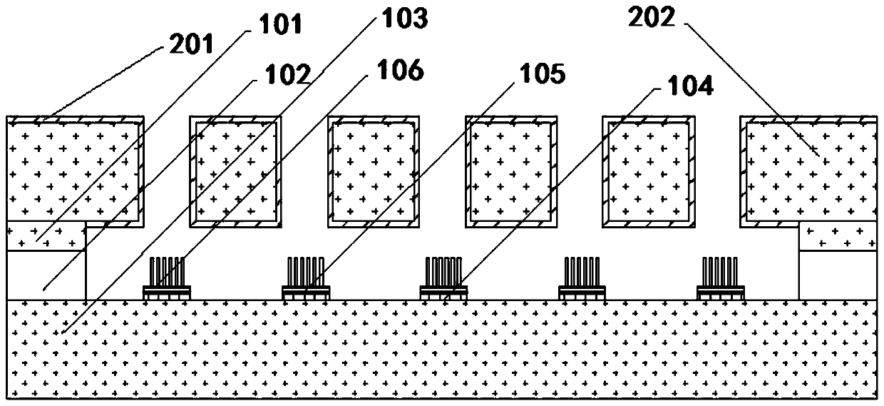
[0035] The manufacturing method of the field emission ion neutralizer chip based on SOI technology among the present invention, generally speaking, comprises the steps:

[0036] 1. Use the bottom silicon 103 in the surface-polished SOI silicon wafer as the cathode base, and the bottom silicon 103 adopts high doping (because the doping method is uncertain, the present invention uses the electrica...


PUM

PropertyMeasurementUnit
Thicknessaaaaaaaaaa
Thicknessaaaaaaaaaa

Abstract

The invention discloses a manufacturing method of a field emission ion neutralizer chip based on an SOI process. The manufacturing method comprises the following steps: (1) preparing an SOI substratewith a polished surface; (2) removing the top silicon and the silicon dioxide insulating layer in the target area by using photoetching and etching processes, and exposing the bottom silicon; (3) obtaining an array type photoresist pattern on the underlying silicon, and depositing a buffer layer and a catalyst layer to form a buffer layer-catalyst layer array; (4) forming a carbon nanotube array to obtain a cathode part; (5) preparing an array type through hole structure by using a silicon wafer as a grid substrate; (6) depositing a metal film on the through hole structure to obtain an anode part; and (7) bonding the cathode part and the anode part to obtain the field emission ion neutralizer chip. By improving the design and the like of the whole flow process of the preparation method, the obtained device can effectively overcome the field shielding effect and the heat effect, and has the advantages of being good in emission efficiency, low in power consumption and long in service life.

Description

technical field [0001] The invention belongs to the technical field of aerospace vehicle electric propulsion, and more specifically relates to a manufacturing method of a field emission ion neutralizer chip based on an SOI process. Background technique [0002] The development of the aerospace field is inseparable from breakthroughs in propulsion technology. At present, a series of aerospace exploration experiments proposed by the state have put forward higher requirements for electric propulsion technology. Electric propulsion has become an important means to improve the overall performance and technical level of spacecraft. For the currently widely used micro-satellites, a micro-electric propulsion system with high-precision micro-new level thrust is needed to realize satellite orbit positioning and attitude control. The micro electric propulsion system can be divided into the following three parts like the traditional electric propulsion system: high-voltage ionization sy...

Claims


Application Information

Patent Timeline
IPC IPC(8): B81C1/00B81C3/00B81B7/00B81B7/02B82Y40/00F03H1/00
CPCF03H1/0025H01J3/022H01J9/025
Inventor 肖东阳孙雷蒙涂良成宋培义匡双阳王玉容
Owner HUAZHONG UNIV OF SCI & TECH
Why Eureka
Try Eureka