A kind of perfect absorber coating and preparation method thereof

A perfect absorption and coating technology, applied in the field of nanomaterials, can solve the problems of time-consuming, difficult to prepare in a large area, and achieve the effect of simple process, reduced preparation difficulty and good absorption effect.

Active Publication Date: 2020-12-11
NINGBO INST OF MATERIALS TECH & ENG CHINESE ACADEMY OF SCI
View PDF9 Cites 0 Cited by
  • Summary
  • Abstract
  • Description
  • Claims
  • Application Information

AI Technical Summary

Problems solved by technology

[0006] Constrained by the nanostructure size, metamaterial perfect absorbers face challenges in realizing broadband perfect absorption, especially in the visible and near-infrared ranges
At present, most of the metamaterial broadband absorbers that have been designed and prepared rely on expensive manufacturing processes, such as electron beam lithography, focused ion beam etching, laser direct writing, etc., which are not easy to prepare in large areas and are very time-consuming.

Method used


Image

  • A kind of perfect absorber coating and preparation method thereof
  • A kind of perfect absorber coating and preparation method thereof
  • A kind of perfect absorber coating and preparation method thereof

Examples


Embodiment 1

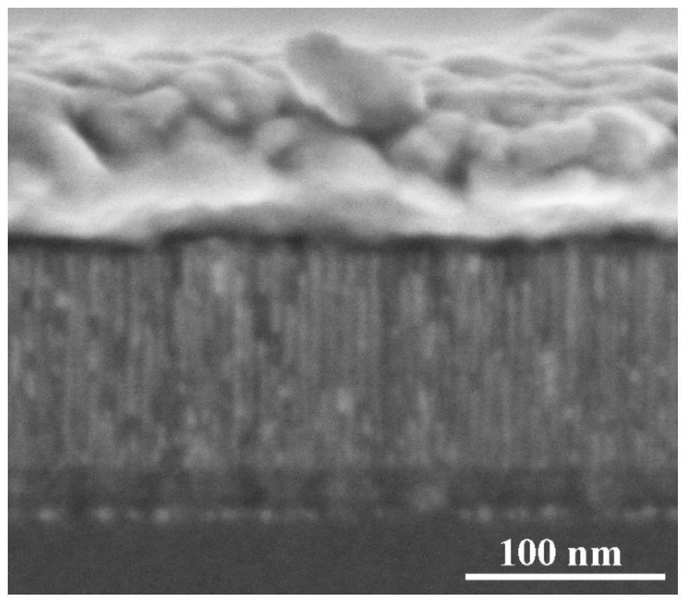
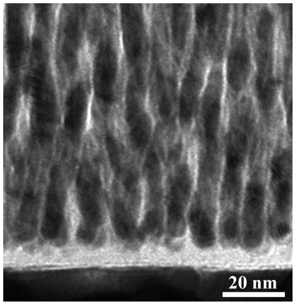
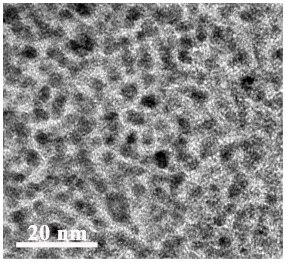
[0055] Put the silicon wafer and quartz wafer into acetone, ethanol and deionized water in sequence, and ultrasonically clean them for 15 minutes to remove surface pollutants; dry the cleaned silicon wafer and quartz wafer with nitrogen, and fix them on the substrate tray; put the tray into into the deposition chamber of the magnetron sputtering equipment, pre-evacuated to 10 -4 Below Pa; feed argon gas to keep the pressure in the deposition chamber at 0.4Pa, clean the tungsten target and alumina target by radio frequency sputtering for 10 minutes, and apply the substrate bias to clean the substrate for 5 minutes; after etching and cleaning, adjust The airflow makes the deposition chamber pressure to 0.3Pa, turn off the alumina target power, open the baffle in front of the tungsten target, start sputtering, adjust the sputtering power density of the tungsten target to 3.5W / cm 2 , deposit the metal layer, and the deposition time is 25 minutes. Turn off the driving power of the...

Embodiment 2

[0059] Clean the silicon wafer and quartz wafer sequentially with acetone, ethanol and deionized water for 15 minutes respectively to remove surface pollutants; dry the cleaned silicon wafer and quartz wafer with nitrogen, and fix them on the substrate tray; put the tray into In the deposition chamber of the magnetron sputtering equipment, simultaneously pre-evacuate to 10 -4 Below Pa; pass argon gas flow to keep the pressure of the deposition chamber at 0.4Pa, clean the gold target and silicon dioxide target by radio frequency sputtering for 10 minutes, and apply a bias voltage to clean the substrate for 5 minutes; after the etching and cleaning, adjust the deposition chamber When the pressure reaches 0.3Pa, turn off the power supply of the silicon dioxide target, open the baffle in front of the gold target, start sputtering, and adjust the sputtering power density of the gold target to 3.5W / cm 2 , deposit the metal layer, and the deposition time is 25 minutes. Turn off the ...

Embodiment 3

[0062]Ultrasonic clean the PET sheet with detergent and deionized water for 10 minutes respectively to remove surface pollutants; dry the cleaned PET sheet with nitrogen and fix it on the substrate tray; put the tray into the deposition chamber of the magnetron sputtering equipment , while pre-evacuating to 10 -4 Below Pa; pass argon gas flow to keep the pressure of the deposition chamber at 0.4Pa, clean the silver target with DC sputtering, and clean the silicon dioxide target with RF sputtering for 20 minutes; after etching and cleaning, adjust the pressure of the deposition chamber to 0.25 Pa, turn off the silicon dioxide target power, open the baffle in front of the silver target, start sputtering, adjust the sputtering power density of the silver target to 2.8W / cm 2 , deposit the metal reflective layer, the deposition time is 30min. Turn off the driving power of the silver target, and start the driving power of the silicon dioxide target at the same time, and set the pow...


PUM

PropertyMeasurementUnit
diameteraaaaaaaaaa
heightaaaaaaaaaa
diameteraaaaaaaaaa

Abstract

The invention discloses a perfect absorber coating. The perfect absorber coating sequentially comprises a metal reflection layer, a dielectric layer, a metal nanowire array-ceramic composite layer, ametal nanoparticle-ceramic composite layer and a dielectric antireflection layer from a substrate to the outside, wherein in the metal nanowire array-ceramic composite layer, metal nanowire arrays aredistributed in ceramic phases in a perpendicular mode, the diameter of each metal nanowire is not less than 3.5 nm, the height of each metal nanowire is equal to the thickness of the metal nanowire array-ceramic composite layer, the distance between every two adjacent metal nanowires is 1-15 nm, the metal nanowires account for 20% to 60% of the volume of the metal nanowire array-ceramic compositelayer, in the metal nanoparticle-ceramic composite layer, metal nanoparticles are uniformly dispersed in ceramic phases, the diameter of each metal nanoparticle is 4-15 nm, and the metal nanoparticles accounts for 5% to 45% of the volume of the metal nanoparticle-ceramic composite layer. The invention further discloses a preparation method of the perfect absorber coating.

Description

technical field [0001] The invention belongs to the field of nanometer materials, and in particular relates to a perfect absorber coating and a preparation method thereof. Background technique [0002] As a new type of electromagnetic metamaterial, the metamaterial perfect absorber has attracted close attention in recent years in thermal emission, optical sensing, and photoelectric detection due to its absorption rate of more than 90% in certain spectral ranges. , which has broad application prospects in the fields of solar cells, military radar stealth, infrared detection, and thermal radiation control. Among them, narrow-band absorbers can be used in the fields of selective thermal radiators and biosensing, while in the fields of solar energy harvesting, seawater desalination, and military stealth, absorbers are required to have excellent absorption characteristics in a wide spectral range. [0003] Common narrow-band absorber structures are MIM structures or MI structure...

Claims


Application Information

Patent Timeline
Patent Type & Authority Patents(China)
IPC IPC(8): C23C14/14C23C14/06C23C14/35
CPCC23C14/06C23C14/14C23C14/3492C23C14/352
Inventor 高俊华臧睿曹鸿涛胡海搏
Owner NINGBO INST OF MATERIALS TECH & ENG CHINESE ACADEMY OF SCI
Why Eureka
Try Eureka