Method for preparing CZTS thin film solar cell using group IIIA element doped cadmium sulfide film

A technology of thin-film solar cells and group elements, which is used in circuits, electrical components, and final product manufacturing, etc., can solve problems such as the photoelectric conversion performance of devices, and achieve the effects of improving device efficiency, widening the width of depletion region, and improving photoelectric performance.

Inactive Publication Date: 2019-08-09
CENT SOUTH UNIV
View PDF2 Cites 6 Cited by
  • Summary
  • Abstract
  • Description
  • Claims
  • Application Information

AI Technical Summary

Problems solved by technology

Although the CdS material has good photoelectric performance, the pure CdS material itself has some shortcomings, which makes the devices made from it have problems in the photoelectric conversion performance.

Method used


Image

  • Method for preparing CZTS thin film solar cell using group IIIA element doped cadmium sulfide film

Examples


Embodiment 1

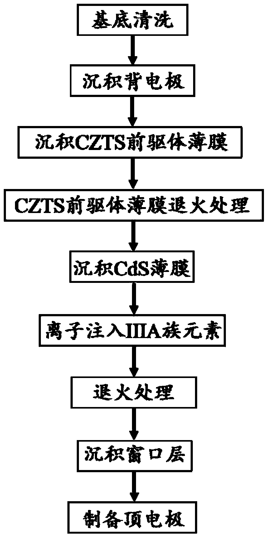
[0029] Please refer to figure 1 , according to the following steps to prepare CZTS thin film solar cells.

[0030] (1) Cut the soda-lime glass into a square of 3mm*3mm, ultrasonically clean it with deionized water, glass cleaner, acetone, alcohol, and deionized water for 15 minutes, and then dry it with a nitrogen gun.

[0031] (2) DC magnetron sputtering double-layer molybdenum was used as the back electrode on the cleaned soda-lime glass, and the thickness of the sputtered film was about 1 μm.

[0032] The sputtering power is 100W, and double-layer Mo is coated, that is, sputtering at 2Pa ​​working pressure for 5 minutes to improve the bonding force with the glass substrate, and then sputtering at 0.3Pa working pressure for 15 minutes to obtain good electrical properties. The sheet resistance of the obtained Mo-coated glass is about 1.2Ω / □.

[0033] (3) The CZTS precursor film was deposited by sol-gel method.

[0034]Add copper acetate (1.6M), zinc acetate (1.0M), tin dic...

Embodiment 2

[0048] (1) Cut the FTO conductive glass into a square of 3mm*3mm, ultrasonically clean it with deionized water, glass cleaner, acetone, alcohol, and deionized water for 15 minutes, and then dry it with a nitrogen gun.

[0049] (2) Metal molybdenum was prepared as the back electrode on the cleaned soda-lime glass by thermal evaporation method.

[0050] Evaporation time 20min, vacuum degree 2×10 -5 Pa, evaporation current 90A, evaporation voltage 1.2V.

[0051] (3) The CZTS precursor film was prepared by continuous ion layer adsorption method, in which the ion layer was ZnS film and Cu 2 SnS 3 film.

[0052] Cu 2 SnS 3 Thin film deposition process: 0.005M CuSO 4 , 0.02M SnSO 4 and 0.01M NH 4 The mixed solution of F is the cation precursor solution, 0.01M Na 2 S is an anion precursor solution; ZnS film deposition process: 0.05M ZnSO 4 The solution is a cationic precursor solution, 0.01M Na 2 S is an anion precursor solution. The immersion and cleaning times during the...

Embodiment 3

[0066] (1) Cut the ITO conductive glass into a square of 3mm*3mm, ultrasonically clean it with deionized water, glass cleaner, acetone, alcohol, and deionized water for 15 minutes, and then dry it with a nitrogen gun.

[0067] (2) DC magnetron sputtering double-layer molybdenum was used as the back electrode on the cleaned soda-lime glass, and the thickness of the sputtered film was about 1 μm.

[0068] The sputtering power is 100W, and double-layer Mo is coated, that is, sputtering at 2Pa ​​working pressure for 5 minutes to improve the bonding force with the glass substrate, and then sputtering at 0.3Pa working pressure for 15 minutes to obtain good electrical properties. The sheet resistance of the obtained Mo-coated glass is about 1.2Ω / □.

[0069] (3) The CZTS precursor film was deposited by sol-gel method.

[0070] Add copper acetate (1.6M), zinc acetate (1.0M), tin dichloride (0.8M) and thiourea (6.4M) to ethylene glycol methyl ether, the metal ratio is Cu / (Zn+Sn)= 0.84...


PUM

PropertyMeasurementUnit
diameteraaaaaaaaaa
thicknessaaaaaaaaaa

Abstract

The invention discloses a method for preparing a CZTS thin film solar cell using a group IIIA element doped cadmium sulfide film. The method comprises the steps of: cleaning a substrate; depositing metal molybdenum as a back electrode on the cleaned substrate; depositing a CZTS precursor film on the back electrode; annealing the CZTS precursor film to obtain a CZTS absorbing layer film; depositinga CdS film on the CZTS absorbing layer film, and doping the CdS film with a group IIIA element by ion implantation; and annealing the sample doped with CdS, then depositing a window layer on the doped CdS; preparing a top electrode on the window layer to obtain the CZTS thin film solar cell. Doping the Group IIIA element can improve the photoelectric performance of CdS, increase the width of a depletion region, and ensure high long-wave collection efficiency and photoelectric conversion efficiency. The ion implantation method can precisely control the concentration and depth distribution of the implanted ions, and the implanted layer does not peel off.

Description

technical field [0001] The invention relates to the technical field of battery thin film manufacturing, in particular to a method for preparing a CZTS thin film solar cell that adopts IIIA group element doping cadmium sulfide thin film. Background technique [0002] With the continuous acceleration of industrialization, energy crisis and environmental degradation are two major problems in the development of the world today. At present, the energy used for human production and life is mainly traditional energy (petroleum, coal, natural gas, etc.), but due to its own characteristics and over-exploitation, traditional energy is gradually exhausted, and will not be able to meet human development needs in the future. Therefore, the development of renewable energy has become an urgent problem to be solved. In essence, traditional fossil fuels are solar energy stored in the form of chemical energy, while wind energy, water energy, and ocean temperature difference energy are solar ...

Claims


Application Information

Patent Timeline
Patent Type & Authority Applications(China)
IPC IPC(8): H01L21/02H01L21/40H01L21/425H01L31/18
CPCH01L21/02557H01L21/02664H01L21/40H01L21/425H01L31/18Y02P70/50
Inventor 韩璐刘芳洋蒋良兴贾明
Owner CENT SOUTH UNIV
Why Eureka
Try Eureka